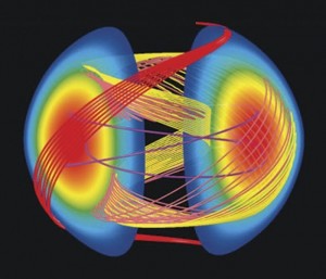
Light that moves and molds gels
Researchers at the University of Pittsburgh have demonstrated a biomimetic response in hydrogels—a material that constitutes most contact lenses and microfluidic or fluid-controlled technologies. Their study, published in Advanced Functional Materials, is the first to show that these gels can be both reconfigured and controlled by light, undergoing self-sustained motion—a uniquely biomimetic behavior. Using computer modeling, the Pitt team demonstrated that the gels “ran away” when exposed to the light, exhibiting direct, sustained motion. The team also factored in heat—combining the light and local variations in temperature to further control the samples’ motions. Controlling a material with light and temperature could be applicable for regulating the movement of a microscopic “conveyor belt” or “elevator” in a microfluidic device. The team also demonstrated that the gels could undergo dynamic reconfiguration, meaning that, with a different combination of lights, the gel could be used for another purpose.
Stanford scientists break record for thinnest light-absorber
Scientists at Stanford University (Stanford, Calif.) have created the thinnest, most efficient absorber of visible light on record. Thousands of times thinner than an ordinary sheet of paper, the invention could lower the cost and improve the efficiency of solar cells, according to the scientists. “Our results show that it is possible for an extremely thin layer of material to absorb almost 100 percent of incident light of a specific wavelength,” says researcher Stacey Bent, professor of chemical engineering. Thinner solar cells require less material and therefore cost less. The challenge for researchers is to reduce the thickness of the cell without compromising its ability to absorb and convert sunlight into clean energy. The next step for the Stanford team is to demonstrate that the technology can be used in actual solar cells.
Scientists solve puzzle of popular photocatalyst
Scientists at University College of London (England) have cleared up a decades-old misunderstanding about how mixed-phase titania photocatalysts operate. Since the 1970s, scientists have known that titania is a photocatalyst—a substance that can break down water and other substances on its surface when it is exposed to light. This property, combined with the fact that titania is cheap and abundant, have made it a widely studied and used substance. Using computational simulations alongside precise experimental measurements of physical samples of the mineral, the researchers found that the widely accepted explanation for how mixed-phase (combined rutile and anatase) titania catalysts operate was misguided. The UCL scientists discovered the precise nature of how band alignment—the relationship between the energy levels of electrons within the material—was the key to the synergystic catalytic capability of mix-phased titania materials.
Nanoscale indenter for thin-film hardness measurement
Researchers from the National Institute of Standards and Technology (NIST; Gaithersburg, Md.) and the University of North Carolina have demonstrated an “instrumented nanoscale indenter” that makes sensitive measurements of the mechanical properties of thin films ranging from auto body coatings to microelectronic devices to biomaterials. The instrument is a touchless surface detector that uses a pair of tiny quartz tuning forks similar to those used to keep time in most wrist watches. When the tuning forks get close to the test surface, the influence of the nearby mass changes their frequency—not much, but enough. The nanoindenter uses that frequency shift to “lock” the position of the indenter mechanism at a fixed distance from the test surface, but without exerting any detectable force on the surface itself. The instrument can measure tip penetration up to 10 μm to within about 0.4 nm, and can be traceably calibrated against basic SI units for force and displacement in a routine manner.
FEI introduces three new TEM systems
FEI introduced three new systems that tailor the power of transmission electron microscopy (TEM) to specific application and industry needs. The new systems provide efficient and effective application-specific workflows for semiconductor manufacturing and scientific research. They include the new Metrios TEM for advanced semiconductor manufacturing metrology, Talos TEM that provides high-speed imaging and analysis for materials and life sciences applications, and the Titan Themis TEM for enhanced atomic-scale measurements of material properties. The Metrios system is the first TEM dedicated to providing the fast, precise measurements that semiconductor manufacturers need to develop and control their wafer fabrication processes. The Talos TEM combines high-resolution, high-throughput TEM imaging with fast, precise and quantitative energy dispersive x-ray analysis to deliver advanced analytical performance with class-leading value. The Titan Themis TEM extends FEI’s leadership position in aberration-corrected, atomic-scale imaging and analysis.

