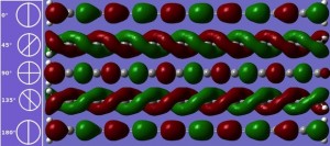
Highest-energy stable form of carbon predicted
Diamond, fullerenes, graphene, carbyne? Using first-principles calculations, scientists at Rice University have determined that the latest form of carbon will be the strongest of a new class of nanomaterials—if and when anyone can make it in bulk. Carbyne (illustrated in the graphic above; credit: V. Artyukhov/Rice Yakobson Group) is a chain of carbon atoms held together by either double or alternating single and triple atomic bonds. In a recent paper in ACS Nano, the researchers explain that the carbon-atom chains would be difficult to make but would have tensile strength and stiffness double that of graphene and an electronic band gap that can be significantly altered by stretching or twisting. They say the carbyne chains can take on side molecules that may make them suitable for energy storage. Based on calculations, carbyne might be the highest energy state for stable carbon, they add.
Iron-oxide-coated ‘nanonets’ catalyze water-splitting reaction
Coating a lattice of tiny wires called nanonets with iron oxide produces an economical and efficient platform for generating hydrogen via water splitting, Boston College researchers reported recently in the online edition of the Journal of the American Chemical Society. The scientists coated titanium disilicide nanowires with hematite and measured increased light absorption efficiency without a precious metal catalyst. According tot the researchers, nanonets serve a dual role as a structural support and an efficient charge collector, allowing for maximum photon-to-charge conversion.
Color X-ray camera provides elemental analysis
A new color X-ray camera at the Helmholtz-Zentrum Dresden-Rossendorf will allow scientists at Helmholtz Institute Freiberg for Resource Technology (HIF), part of HZDR, to quickly determine the concentrations of very finely dispersed metals in ores, including rare-earth elements. Rare-earths such as neodymium and cerium are dispersed very finely and in small quantities, and the camera is said to allow precise analysis of both the chemical and spatial composition of ore samples using a proton beam that is evenly directed onto the entire sample. The protons generate X-rays indicating what elements are present, and the camera simultaneously creates an optical image using a lens containing capillary optics. So far, these types of cameras have only been operated at larger synchrotron systems for applications other than raw materials analysis, according to the researchers.
X-ray tomography shows why lithium–ion batteries fail
Materials in lithium–ion battery electrodes expand and contract during charge and discharge, resulting in particle fracture and reduced battery life. Scientists at the Swiss Federal Institute of Technology in Zurich say they recently studied and quantified the effect by using high-resolution 3D X-ray tomography movies recorded while the batteries were in operation. Using synchrotron radiation, the researchers observed the inside of a Li–ion battery as it charged and discharged over 15 hours, capturing the degradation mechanisms occurring in the electrode. Tin oxide particles expand during charging due to the influx of lithium ions, then shrink during discharge. However, they undergo permanent deformation that demonstrates that the electrode’s polymer binder is not yet optimized for high volume expansion materials, according to the researchers. The deformation impacts battery performance by causing individual SnO particles to become disconnected from the electrode and reducing battery capacity. Results of the study will be published in the journal Science.
Process said to make 2 million nanowires in 2 hours
Members of a South Korean industrial/academic research team say they have developed technology that could commercialize production of nanowires from an array of materials. Scientists from LG Innotek and the Korea Advanced Institute of Science and Technology applied semiconductor processing methods to nanowire production, using a photo-engraving technique to produce a 100-nm linear grid pattern on a 20-cm diameter silicon wafer board. They then used a sputtering process to mass-produce up to two million nanowires 50 nm wide and up to 20 cm in length. The technology requires neither a lengthy synthesis process nor post-cleaning, the researchers say. Wire materials included metal, dielectric, oxide, and ferroelectric materials. Results of the work were published online in a recent edition of Nano Letters.

