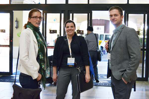
![0122ctt ema DSC_0724 opening plenary lo res[3]](https://ceramics.org/wp-content/uploads/2015/01/0122ctt-ema-DSC_0724-opening-plenary-lo-res3.jpg "0122ctt ema DSC_0724 opening plenary lo res[3]")
[Image credit] ACerS
The Spanish explorer Ponce de León named America’s panhandle La Florida, a name that means “place of flowers.” And he was right.
I’m at the ACerS Electronic Materials and Applications 2015 in sunny Orlando, Fla., this week, and as I look around, I’m can’t help but think that rascal Ponce knew what he was talking about—there are lush green plants and vibrant colored flowers everywhere, making me completely forget the despair-filled gray landscape of the Midwest that I escaped from just a few days ago.
Although the scenery is flowery, however, that’s about where my analogy stops. The technical language happening at EMA 2015 is anything but flowery, but no less impressive.
EMA 2015 kicked off on Wednesday morning with the first plenary talk delivered by Kent Budd, senior staff scientist at 3M’s Corporate Research Materials Laboratory (St. Paul, Minn.). Budd’s talk, “EMA related technologies and research at a diverse global manufacturer,” provided a sneak glimpse into many different areas of research and development going on at 3M. As Budd put it, “There are interesting advances going on in materials across the board.”
![0122ctt ema DSC_0733 Kent Budd lo res[3]](https://ceramics.org/wp-content/uploads/2015/01/0122ctt-ema-DSC_0733-Kent-Budd-lo-res3.jpg)
Kent Budd opening up EMA 2015 with the first plenary talk. Credit: ACerS
While the company may be more well-known for its consumer products—Scotch tape and Post-it notes, for example—those products only constitute one of 3M’s five business groups. Another of those groups is comprised of electronic and energy applications. Budd’s talk focused on this group, particularly regarding advances in electrical energy storage and LCD displays.
Budd touched on one of Ceramic Tech Today’s favorite topics, batteries—3M is working on new cathode and anode materials to improve the performance, safety, and cost of lithium-ions. Some of those projects include different configurations and compositions of nickel, manganese, and cobalt (NMC) materials for cathodes and advanced anodes that replace graphite with metals like silicon and tin.
The adventurous scientists at 3M get to have a little fun with their developments, too, in what Budd calls “Does it explode?” tests. (Maybe they were inspired by Mythbusters?) Prototype batteries with tailored NMC compositions have fared well in these tests, Budd showed, as they can provide comparable performance minus the explosive ability of conventional LiCoO2 batteries.
Moving away from energy storage, Budd also touched on LCD technologies, a hot topic from the recent Consumer Electronics Expo. 3M is advancing polarizers in LCD screens, an important yet inefficient part of the screens’ technology. As Budd explained—and we have covered before on CTT—simple polarizers adsorb half the light emitted from a screen, making them rather energy inefficient.
Metal-organic framework (MOF) recirculating polarizers instead repeatedly reflect one polarization, recovering half of the light with each reflection—they essentially bounce light around until it is in the correct polarization and can be emitted. Recirculating polarizers have potential to reduce wasted light and increase the energy efficiency of our most beloved devices, Budd says.
3M is also working on improving touch screens, in an effort to make bigger touch screens that still work as well as those in smartphones and other smaller devices. The tech behind touchscreens is projected capacitive touch sensors, which are limited by available transparent conductors. 3M is exploring patterned metal mesh films, which contain >99% open area for excellent optical transmission, and patterned silver nanowire touch films printed with Cambrios ink as possible transparent conductor candidates that will allow bigger touchscreens in the future.
In short, “Many interesting EMA-related materials are hidden away at 3M,” Budd concluded.
After Budd’s kick-start talk, the conference continued full speed ahead by breaking into a host of concurrent symposia on functional thin films, ion-conducting ceramics, LEDs and photovoltaics, mutliferroic materials, and many more thought-provoking electronic topics.
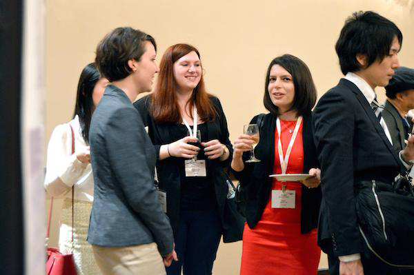
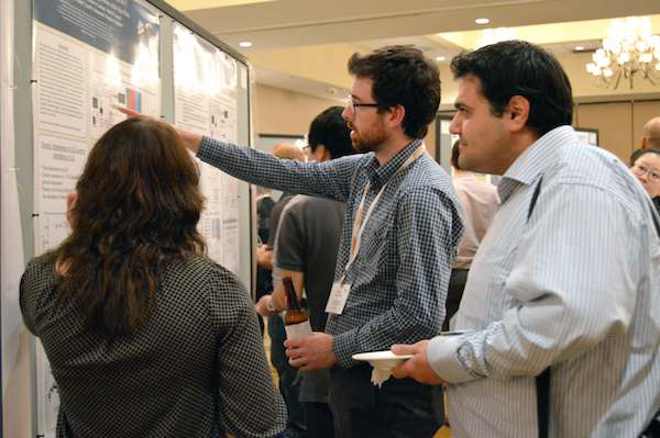
The top eight students finalists for the Best Student Paper Award presented their work in 15-minute talks over lunch on Wednesday and Thursday, providing a snapshot of some of the excellent electronic materials research being done by tomorrow’s leaders. Presentation of great research continued at Wednesday evening’s poster session and reception, where drinks and discussion further fueled the day’s energy.
Travel, a late evening tutorial on thin films, and first night festivities on Wednesday made for some weary faces Thursday morning. But Greg Rohrer, professor and head of the Materials Science and Engineering Department at Carnegie Mellon University (Pittsburgh, Pa.), invigorated the conference’s second day with his plenary talk, “High throughput, data rich experiments and their impact on ceramic science.”

Greg Rohrer delivering the second plenary talk at EMA 2015. Credit: ACerS
Rohrer’s talk focused on advances in combinatorial substrate epitaxy, an alternative to conventional epitaxy studies. Combinatorial substrate epitaxy uses polycrystalline substrates and defined epitaxial film growth to determine grain orientation of a much wider range of substrates than conventional studies allow.
The resulting data from this method is an electron backscatter diffraction (EBSD) map of crystals and grain boundaries depicting orientation of each individual crystal as a different color—a highly informative map that happens to be very pretty, too.
The EBSD maps Rohrer showed depicted materials in vibrant hues of data, their hidden complexity masked by the fact that they looked like multicolored melamine tableware.
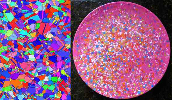
A typical EBSD image (left) (Credit: Q2Q7; Wikimedia Commons), which strangely resembles multicolored melamine tableware (right) (Credit: Lori B. Stalteri; Flickr CC BY 2.0).
Delving deeper into grain boundaries, Rohrer discussed recent advances that allow 3-D microstructure measurements of those boundaries using automated dual-beam focused ion beam (FIB) microscopy.
Rohrer showed a six-second movie of the technique—which compiles two days’ worth of data collection, he says—that alternately uses an ion beam to measure EBSD of a single layer of material and a separate ion beam to etch away a very thin layer of material, exposing a new layer for measurement. This process continues etching and measuring progressive layers through the depth of the material.
The automated process ultimately gathers a bank of data that can be used to reconstruct a 3-D map of the material’s grain boundaries. These technologies are providing new possibilities and widening opportunities for high-throughput, in-depth materials investigations, Rohrer says.
Rohrer concluded his talk by raising a point and posing a challenge to the audience and to the field—for more comprehensive and available digital data archives. Rohrer leads by example, discussing the inspiration for and utility of his own grain boundary data archive, a repository for his group’s digital data.
He hopes providing more open access to this sort of data will not only increase transparency and rigor of studies, but also can provide opportunities for additional experimentation from each dataset. Considering the time and money that goes into one of these studies—or any research study, really—providing the opportunity to test more than one question from each dataset is a wise use of resources.
“I don’t know what the future will bring, but archiving and sharing of digital data will be very important to accelerated development of ceramics,” Rohrer says.
Stay tuned for additional coverage of EMA 2015 on Twitter, the complete cache of photos on Flickr, and a full conference recap on Ceramic Tech Today next week.
Interested in more electronic materials? Download a PDF of the conference program for a full list of titles, topics, attendees, and abstracts.

Credit: ACerS
Credit: ACerS
Credit: ACerS
Credit: ACerS
Credit: ACerS