This award recognizes individuals, whose innovations are at the cusp of commercialization in a field related, at least in part, to ceramics and glasses. This award recognizes a member of the ceramics and glass research community for exceptional discovery or invention(s) that can, or have, led to innovative products and/or processes.
The Rishi Raj Medal for Innovation and Commercialization recognizes individuals, whose innovations are at the cusp or an early stage of commercialization. The innovation should be in a field related, at least in part, to ceramics and glasses.
The confluence of science, manufacturing, and software tools is leading to a new era of innovation and commercialization. Its impact will continue to be felt broadly in how we live, work, travel, and interact with one another and our environment. The endeavors receiving this award are expected to be high risk, but, nevertheless, the potential application of the work should be visionary and purposeful.
This award recognizes a member of the ceramics and glass research community for exceptional discovery or invention(s) that can, or have, led to innovative products and/or processes. Colleagues at all levels of careers in academia, industry and national labs are eligible. Membership in the American Ceramic Society is not required.
The Award is a medal, $2,500 award and registration waiver to attend ACerS Annual Meeting. The award is presented at the ACerS Annual Meeting Awards Banquet. One Medal will be presented each year.
Nomination Process
Nominations should consist of a concise description of the achievement (200 word maximum) that outlines its significance in terms of past, on-going or the potential for societal benefit through science and technology. Up to three one-page supplementary documents (e.g., support letters, pictures or product description) that would aid in the evaluation process should be submitted.
Membership in the Society is not required. However, the nominator should be a member of the American Ceramic Society. Self nominations are permitted.
Nominations not selected will be considered in following years (up to five years).
Award Namesake
The Rishi Raj Medal for Innovation and Commercialization was established through a gift from Rishi Raj. Prof. Raj has made significant contributions to ceramic science and technology. His noteworthy contributions are on the mechanical properties of ceramics, and the processing of oxide and non-oxide ceramics. His research has focused on both powder processing and polymer-derived-ceramics. Most significant recent contribution has been his discovery of flash sintering method for a wide range of ceramics and investigation of the influence of electric fields on defects in ceramics at high temperature.
Contact
Erica Zimmerman
ezimmerman@ceramics.org
Award Winners
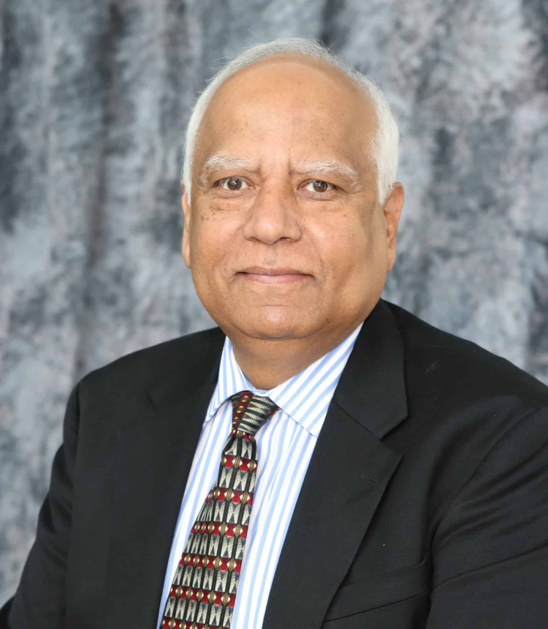
Mrityunjay Singh
Dr. Mrityunjay Singh is Chief Scientist, Ohio Aerospace Institute, Cleveland, OH. He received his Ph.D. in Metallurgical Engineering from Indian Institute of Technology-BHU, India in 1983 and did his post-doctoral work at Louisiana State University, LA and Rensselaer Polytechnic Institute, NY.
Dr. Singh is globally recognized for his long term and outstanding contributions to science and technology of advanced materials and manufacturing technologies. His research has addressed both basic and applied questions and has been instrumental in establishing design, integration, and performance limits for single and multi-materials used in a wide variety of aerospace and ground-based applications.
Dr. Singh is ACerS Past President and currently President of World Academy of Ceramics, Italy. He is a Fellow of ACerS, ASM International, American Association for the Advancement of Science (AAAS), Indian Institute of Metals (IIM), and US National Academy of Inventors (NAI). He is Honorary Fellow of European Ceramic Society, Indian Institute of Ceramics, and honorary member of Materials Research Society of India, Indian Ceramic Society, and Distinguished Life Member of Alpha Sigma Mu. He has received Honorary Doctorates from Nagaoka University of Technology, Japan, Slovak Academy of Sciences, Slovakia, and AGH University, Krakow, Poland.
Dr. Singh is recipient of nearly 100 national and international awards including Distinguished Life Membership (DLM) Award, Edward Orton, Jr. Memorial Lectureship Award, W. David Kingery Award, John Jeppson Award, Richard M. Fulrath Award, Samuel Geijsbeek PACRIM International Award, and James I. Mueller Awards from ACerS, and Albert Sauveur Achievement Award and Edward DeMille Campbell Memorial Lectureship from ASM International. He received NASA Public Service Medal, NASA Outstanding Public Leadership Medal, Silver Snoopy Award, Sir Richard Brook Award, Ishikawa International Carbon Prize, and International Dresden Barkhausen Prize and many other awards and honors from all over the world.