
[Image above] Networking in the lobby of the DoubleTree Orlando SeaWorld. Credit: ACerS
The 2016 edition of Electronic Materials and Applications—the meeting’s seventh annual installment—took place this week in sunny Orlando, Fla. [Want to see for yourself? Check out the pictures on our Flickr page!]
EMA is all about electronics—the meeting covers emerging needs, opportunities, and key challenges within the field, highlighting the latest advances in electronics, sensors, energy generation and storage, photovoltaics, and LEDs. ACerS Electronics Division and Basic Science Division jointly program the meeting.
And with more than 300 international attendees (a record attendance!), the conference is sized just right—big enough to feature a variety of high-quality research and countless networking opportunities, yet small enough to get to know your fellow attendees. Those 2016 attendees hailed from diverse locations scattered all across the globe.
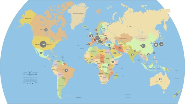
EMA 2016 attendees traveled from around the globe to converge in Orlando. Credit: Haiyan Wang
If you missed this opportunity to present, learn, and network within the electronics community this year—or if you were there and know how valuable the conference is—be sure not to miss EMA 2017, which will return to Orlando, Fla., Jan. 18–20, 2017.
In addition to high-quality technical talks spanning all electronic topics, a buzzing poster reception, expert tutorials, and the not-to-be missed special symposium dedicated to learning from failed research, this conference also consistently delivers incredibly high-quality plenary lectures to get each day humming.
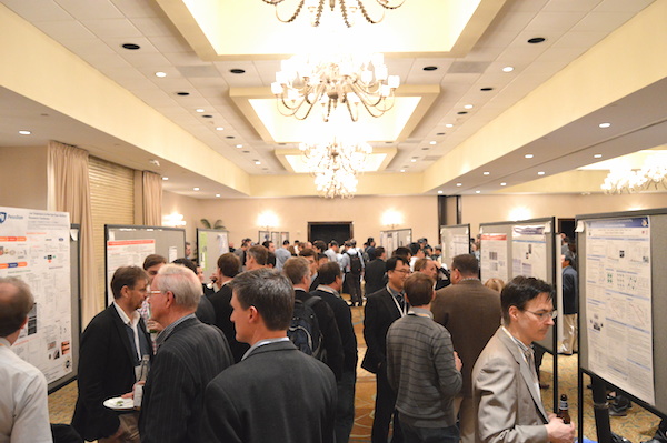
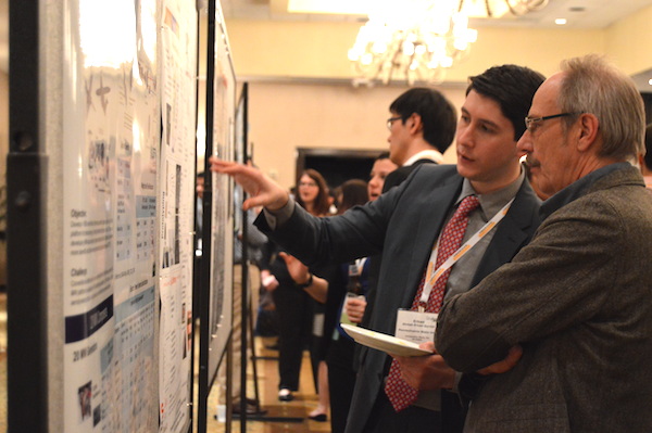
The packed poster session. Credit: ACerS
Day 1—Darrell Schlom
Darrell Schlom’s opening plenary talk Wednesday morning switched on the meeting with a thick discussion of oxide thin films. Schlom put his years of research expertise—most recently at Cornell University (Ithaca, N.Y.) as Herbert Fisk Johnson Professor of Industrial Chemistry—to work.
Schlom showed how “tricks” to generate thin films can uncover interesting properties in otherwise usual materials. However, these engineered thin films often don’t experimentally measure up to theoretical predications of their performance. What gives?
Defects—Schlom demonstrated—lots of them.
Schlom’s Cornell University group has done significant work to show how theoretical models can inform how to pioneer materials design to advantageously engineer these atomic anomalies. Those engineered defects can be leveraged to diversify the properties and potential applications of thin films into all new directions.
Questioning the packed audience, Schlom ended his talk by tantalizing of what’s yet to come. “What hidden ground states await?” he asked.
Day 2—James Warren
James Warren, technical program director for materials genomics at NIST’s Material Measurement Laboratory (Gaithersburg, Md.), delivered the plenary talk Thursday morning, speaking about the Materials Genome Initiative and what NIST is doing to support MGI.
What makes MGI different from other initiatives, Warren says, is its commitment to sharing, partnering, and innovating when it comes to materials science data. So, to deliver on that commitment, NIST is spearheading efforts to enable access to materials data to combat problems with data sharing and management in the current scientific publishing system.
(In case you didn’t click on that last link, I urge you to—Warren woke up the audience with a few early morning laughs when he showed the entertaining video during his talk.)
Those efforts are towards an indexed, searchable, and centralized point to find and access all kinds of materials science data—exactly what NIST has developed with its soon-to-be-launched NIST Materials Resource Registry.
While challenges will undoubtedly remain with such a comprehensive and nuanced data collection, Warren acknowledges that this will be a starting point for a resource intended to evolve into an ever more useful and sophisticated solution to the challenges of sharing and managing materials science data.
Day 3—Thomas Detzel
Finaly, Thomas Detzel, senior manager of gallium nitride technology at Infineon Technologies Austria AG (Villach, Austria), continued the energy on the final day of the meeting with his plenary on power semiconductors.
Power devices, which regulate the flow and conversion of electricity in the electronic devices that are part of our everyday lives, play a huge role in reducing worldwide energy use and moving towards a more sustainable energy future, Detzel says. Infineon is part of that future as one of the leading companies in the power semiconductor market.
One of the ways power devices save energy is by using better suited and more efficient materials, like switching out silicon for gallium nitride.
But although gallium nitride has afforded massive improvements in device efficiency and substantial energy savings, new semiconductor materials are continually needed to enable compact and fast switching devices and afford the utmost efficiency, Detzel says. In other words, more work is needed—which opens ongoing opportunities for symbiotic relationships between academia and industry.
Remember, EMA 2017 will continue the tradition of bringing top-level research and speakers to Orlando, Fla., Jan. 18–20, 2017—don’t miss this opportunity to connect and network with the electronic materials community.
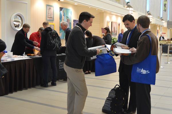
Checking out all the full lineup of technical symposia in the conference program. Credit: ACerS
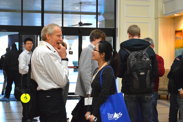
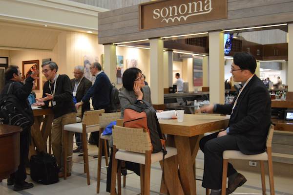
Catching up in the lobby of the DoubleTree Orlando SeaWorld. Credit: ACerS
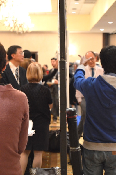
The poster session was abuzz. Credit: ACerS
Poster presenters were met with attendees eager to hear about the latest results. Credit: ACerS
Coffee breaks allow plenty of additional networking opportunities between technical sessions. Credit: ACerS
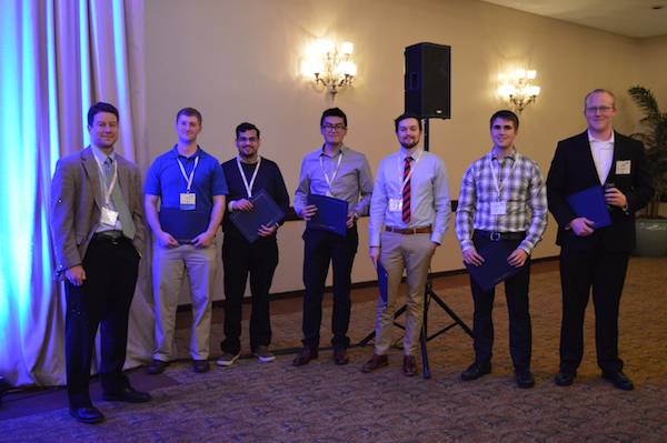
Student award winners at the conference banquet dinner. Credit: ACerS