
[Image above] Solar array. Credit: Nick Blackmer; CC BY-NC-ND 2.0]
Re-imagining efficient solar energy technology is a never-ending exercise in creativity—and scientists continue to “think outside the solar cell” to build on every innovation.
That’s because cost-effective solar power solutions are a crucial part of the equation if we want to divorce ourselves from our reliance on fossil fuels for good.
In the past year, we’ve seen research about how windows-turned-solar-cells could revolutionize energy-efficient buildings; how the key to large-scale solar power storage could be rusting before our eyes; and how perovskites might be the answer to highly efficient, low-cost solar fuel cells.
And solar energy technology continues to make great strides.
Earlier this year, researchers at the Massachusetts Institute of Technology developed a proof-of-concept for solar cells so thin, flexible, and lightweight that they could be placed on almost any material or surface, including your hat, shirt, or smartphone, or even on a sheet of paper or a helium balloon. Although the real deal may be years away from large-scale development, this new approach to making solar cells could be key in powering the next generation of portable electronic devices, the researchers say.
Now scientists at Pennsylvania State University are working on a new high-pressure technique that may allow production of huge sheets of thin-film silicon semiconductors at low temperatures in simple reactors—and they say it can be done for a fraction of the cost of current methods, according to a Penn State news release.
“We have developed a new, high-pressure, plasma-free approach to creating large-area, thin-film semiconductors,” John Badding, leader of the research team and professor of chemistry, physics, and materials science and engineering at Penn State, explains in the release. “By putting the process under high pressure, our new technique could make it less expensive and easier to create the large, flexible semiconductors that are used in flat-panel monitors and solar cells and are the second most commercially important semiconductors.”
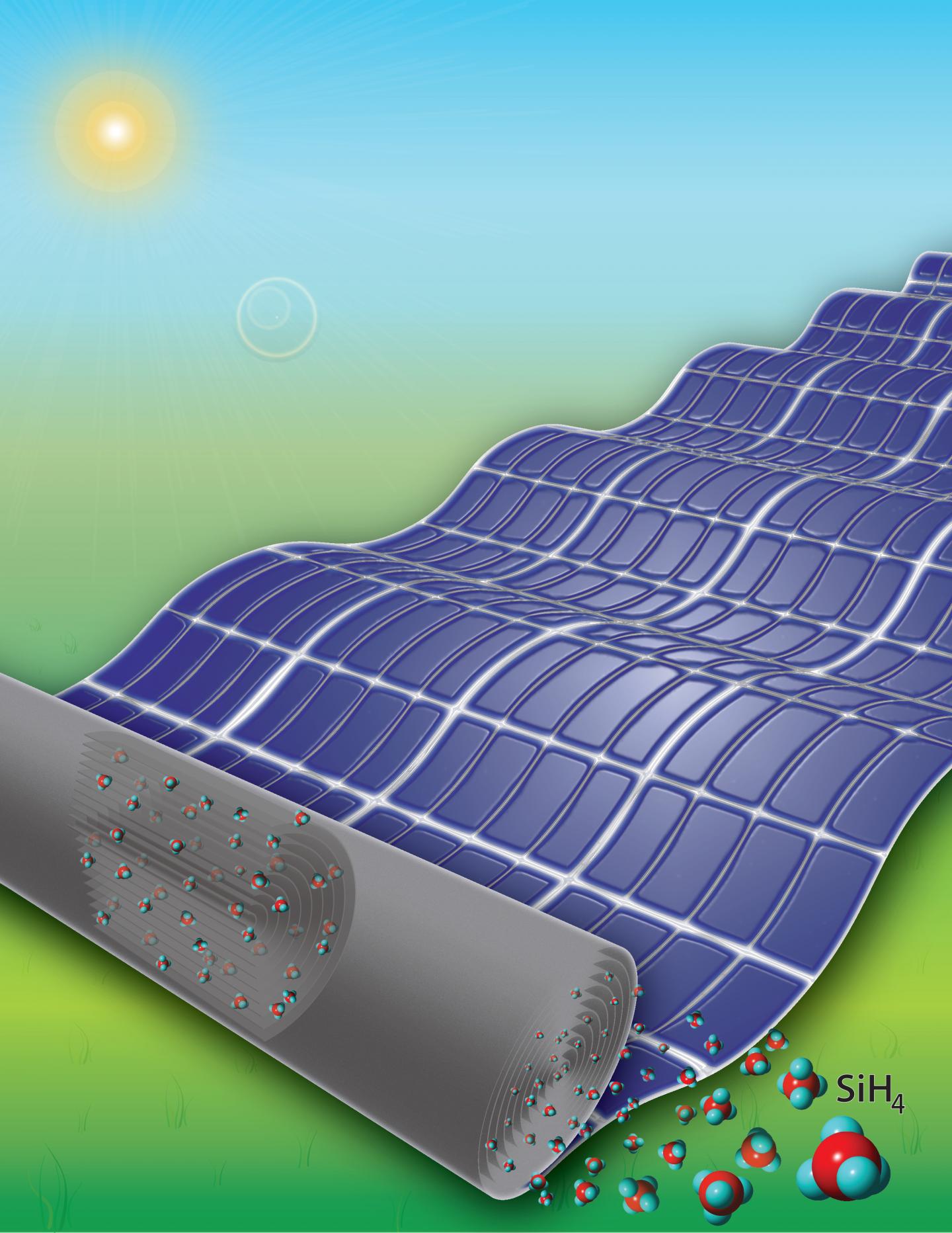
High-pressure deposition inside rolled-up, flexible substrates allows for extremely large-area, uniform-thickness, hydrogenated, amorphous silicon films that are useful for applications such as flat-panel displays and solar cells. Credit: Penn State University
Current methods to make silicon semiconductors use chemical vapor deposition, a process in which silane, a silicon and hydrogen gas, undergoes a chemical reaction to deposit silicon and hydrogen atoms in a thin layer to coat a surface, according to the release. But to create a functioning semiconductor, this chemical reaction needs to happen at a low enough temperature so that hydrogen atoms are retained within the coating. If the temperature is too high, those hydrogen atoms would evaporate away into the air—like steam from boiling water, the release explains.
Current technology can achieve this low-temperature processing, but it’s not cost-effective. The process involves creating plasma—a state of matter similar to a gas that’s made up of ions and free electrons—in a large volume of gas at low pressure. To do this requires huge, expensive reactors to generate the plasma and to accommodate the large volume of gas required, the release explains. And those are difficult to ship.
“With our new high-pressure chemistry technique, we can create low-temperature reactions in much smaller spaces and with a much smaller volume of gas,” Badding adds. “The reduced space necessary allows us, for the first time, to create semiconductors on multiple, stacked surfaces simultaneously, rather than on just a single surface. To maximize the surface area, rolled-up flexible surfaces can be used in a very simple and far more compact reactor. The area of the resulting rolled-up semiconducting material could, upon further development, approach or even exceed a square kilometer.”
The research, published in Advanced Materials, is “High pressure chemical vapor deposition of hydrogenated amorphous silicon films and solar cells” (DOI: 10.1002/adma.201600415).