
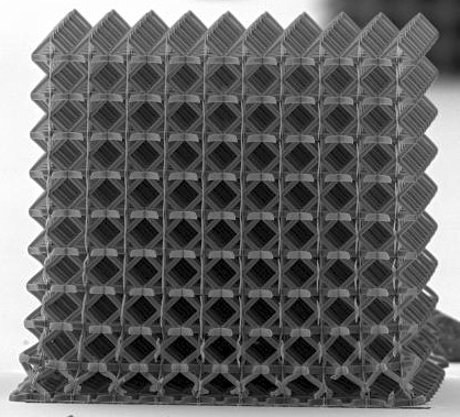
Caltech researchers produced this hollow titanium nitride nanotruss with tessellated octahedral geometry. Each unit cell is on the order of 10 μm, strut length is 3–5 μm, and TiN thickness is roughly 75 nm. (Credit: D. Jang and L. Meza, Caltech.)
Bio-inspired materials ‘made-to-order’
Scientists have long suspected that the tremendous strength of many biological materials has to do with their hierarchical architecture—that is, the way they are built up from different structural elements at the nanometer scale. Engineers at the California Institute of Technology (Caltech; Pasadena) have created nanostructured, hollow ceramic scaffolds from small unit cells that display remarkable strength and resistance to failure despite being more than 85 percent air. The largest structure the team has fabricated thus far is a one-millimeter cube (see photo above). Compression tests on the structure indicate that not only the individual unit cells but also the complete architecture can have unusually high strength, depending on the material, which suggests that the general fabrication technique the researchers developed could be used to produce lightweight, mechanically robust small-scale components such as batteries, interfaces, catalysts, and implantable biomedical devices.
MoS2, gold combine for possible future electronics
Researchers at Kansas State University, Manhattan, have found that adding gold atoms to three-atom-thick molybdenum disulfide improves its electrical characteristics and may advance transistors, photodetectors, sensors, and thermally conductive coatings. It could also produce ultrafast, ultrathin logic and plasmonics devices, the scientists say. The three-atom-thick sheets of MoS2 have recently shown to have transistor-rectification better than graphene. The researchers studied the material’s structure and realized that sulfur groups on its surface had a strong chemistry with noble metals, including gold. They then enhanced several transistor characteristics of MoS2 by manipulating it with gold nanomaterials. The scientists plan to create further complex nanoscale architectures on molybdenum disulfide to build logic devices and sensors.
Light changes material from metal into semiconductor
Scientists at Washington University, St. Louis, Mo., have changed the electronic properties of a new class of materials just by exposing them to light. The research team recently reported work with gold nanorod–zinc oxide composites that led to a “metal-to-semiconductor switching” phenomenon that may enable development of different kinds of sensors and electronic devices. The scientists coated gold nanorods with a thin (10-nm) film of zinc oxide. When exposed to light, the composite changed from a material with metallic properties into a semiconductor. The scientists say exposing the gold nanorods to light causes electrons to flow to the zinc oxide film, which then starts to conduct electricity. They hope to develop a better understanding of the charge conduction mechanism and determine what effects exposure to different wavelengths of light may have on the phenomenon.
Research to investigate kesterite materials for thin-film photovoltaics
With a total budget of more than €3.7 million, a new European research project will focus on development of kesterite-based thin-film solar cells. Kesterites are quaternary/pentenary compounds with a crystal structure very similar to that of chalcopyrites currently used to produce CIGS solar cells. According to researchers working on the KestCells project, the materials may offer a low-cost thin-film PV alternative to CIGS, which rely on relatively scarce indium. In addition to developing new technologies to improve the cost, efficiency, sustainability, and producibility requirements needed for solar PV to become a reliable alternative to nonrenewable energy sources, the project will also focus on creating an international network for training of researchers in advanced thin-film PV technologies.
Low-temp technique for producing thin-film germanium
(Azonano.com) Using gold as a catalyst, scientists at Kyushu University (Japan) have grown germanium crystals at about 250°C with the proper orientation and electrical properties necessary for electronic applications. Unlike other methods, the approach does not require high temperatures or other crystals to act as nucleation points to grow the germanium crystal. And, the researchers say, the new method can be used to produce germanium films with a very large area, allowing for more potential applications. Because charged particles move through germanium more readily than they do through silicon, it is a good candidate material for thin-film transistors needed for flexible and other next-generation electronics applications. The need for high temperatures in germanium film growth, however, has limited their possible use in thin-film applications.