
[Image above] Does silicon’s reign in the electronics world have an expiration date? Credit: Oliver Hammond; Flickr CC BY-NC-SA 2.0
If it weren’t for oxygen—that reactive little eight-proton, infomercial-inspiring number—silicon would hold top spot as the most abundant element (by mass) in our planet’s crust—but I suppose second place is nothing to scoff about.
Silicon is a unique element with a lucky collection of characteristics thanks to its atomic makeup. In it’s pure form, the element is an insulator. But dope it with a small amount of impurities and you can make silicon an interesting and quasi-good conductor—a semiconductor.
Silicon is the life of the semiconductor party. (Not to be confused with silicone, a polymer that contains silicon, which can be the life of a different kind of party.) Because it’s not too insulating and not too conducting, silicon has found itself the almost exclusive force behind today’s electronics.
But silicon is not without its limits, especially with the ever-increasing speed and ever-decreasing size requirements in today’s components—we want our gadgets to be smaller, run faster, and do more.
Silicon can only do so much, however, and the wonder material is quickly approaching its limits. As we’ve already read, silicon might soon be losing ground to perovskites when it comes to both solar cells and LED lights. And other materials are also quickly entering the race to replace silicon, too.
Researchers at the University of Cambridge, A*STAR Data-Storage Institute in Singapore, and the Singapore University of Technology and Design are looking to phase-change materials to potentially bump silicon from the semiconductor top spot.
According to a Cambridge press release, these new devices could potentially fast-forward processing speeds by 500–1,000 times that of the average current laptop computer.
“Currently, the smallest logic and memory devices based on silicon are about 20 nanometres in size—approximately 4,000 times thinner than a human hair—and are constructed in layers,” the release continues. “As the devices are made ever smaller in order to increase their numbers on a chip, eventually the gaps between the layers will get so small that electrons which are stored in certain regions of flash non-volatile memory devices will be able to tunnel out of the device, resulting in data loss. Phase-change material devices can overcome this size-scaling limit since they have been shown to function down to about two nanometres.”
The new research, published in Proceedings of the National Academy of Sciences, uses chalcogenide glass to create novel devices. The material can be melted and recrystallized very quickly—down to a nanosecond—which allows these phase change materials to switch rapidly between a conductive crystalline state and an insulating glassy state. Compared to silicon-based devices, where logic and memory applications are separate, phase-change materials allow these two functions to coexist in the same area, greatly speeding up processing while also using less energy (bonus!).
“Ideally, we’d like information to be both generated and stored in the same place,” lead author Desmond Loke says in the release. “Silicon is transient: the information is generated, passes through and has to be stored somewhere else. But using phase-change material logic devices, the information stays in the place where it is generated.”
“Eventually, what we really want to do is to replace both DRAM and logic processors in computers by new PCM-based non-volatile devices,” senior author Stephen Elliott adds. “But for that, we need switching speeds approaching one nanosecond. Currently, refreshing of DRAM leaks a huge amount of energy globally, which is costly, both financially and environmentally. Faster PCM switching times would greatly reduce this, resulting in computers which are not just faster, but also much ‘greener’.” (Elliot was the Morey Award lecturer at the DGG–GOMD conference in May.)
The paper is “Ultrafast phase-change logic device driven by melting processes” (DOI: 10.1073/pnas.1407633111).
In another scheme to topple silicon’s reign, researchers at Harvard say that correlated oxides can compete with the best of silicon transistors.
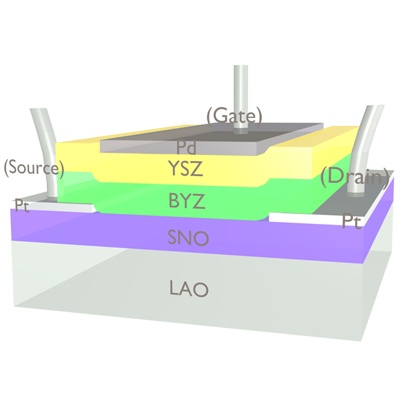
The team, led by materials science professor and ACerS member Shriram Ramanathan, fabricated a correlated oxide transistor primarily of samarium nickelate that achieves an on/off ratio (a measure of how well the material can switch between conductive states) that is greater than 105—far exceeding the previous performance of correlated oxides, which only achieved ratios up to 102—which is on par with silicon transistors.
Schematic of a new correlated transistor made primarily of samarium nickelate. Credit: Jian Shi; Harvard U.
According to a Harvard press release, the research is “an important proof of concept,” and future research will look at the functionality of the device—its switching dynamics and power dissipation.
“Our orbital transistor could really push the frontiers of this field and say, you know what? This is a material that can challenge silicon,” Ramanathan says in the release.
To achieve these impressive characteristics, the researchers nudged the material’s band gap. “By a certain choice of dopants—in this case, hydrogen or lithium—we can widen or narrow the band gap in this material, deterministically moving electrons in and out of their orbitals,” Ramanathan says. The release continues: “That’s a fundamentally different approach than is used in other semiconductors. The traditional method changes the energy level to meet the target; the new method moves the target itself.” Ramanathan used similar band gap manipulation to make a vanadium oxide-based perfect light absorber a few years ago.
One of the benefits to correlated oxides is that they are quantum materials. ““If you have two electrons in adjacent orbitals, and the orbitals are not completely filled, in a traditional material the electrons can move from one orbital to another,” Ramanathan continues. “But in the correlated oxides, the electrons repulse each other so much that they cannot move. The occupancy of the orbitals and the ability of electrons to move in the crystal are very closely tied together—or ‘correlated.’ Fundamentally, that’s what dictates whether the material behaves as an insulator or a metal.”
The paper, published in Nature Communications, is “Colossal resistance switching and band gap modulation in a perovskite nickelate by electron doping” (DOI: 10.1038/ncomms5860).
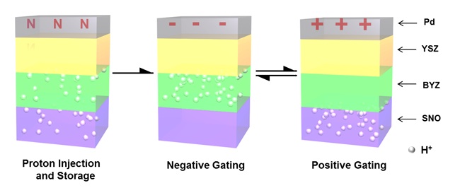
During fabrication, the annealing process injects hydrogen ions into thin films of samarium nickelate (SNO) and yttrium-doped barium zirconate (BYZ). During operation, an electric field moves the charges from one layer to the other, and the influx or loss of electrons modulates the band gap in the SNO, resulting in a very dramatic change in conductivity. Credit: Jian Shi; Harvard U.