
This video from the Graphene Flagship explains graphene basics. Credit: Graphene Flagship.
Graphene is big—well, actually, it’s really small. But in a really big way.
Graphene is so big, in fact, that the European Commission early last year commenced the Graphene Flagship, a 10 year, €1B initiative to advance collaborative research by between academia and industry to initiate novel research efforts to push graphene onto the factory floor. Watch the three-minute video above from the Graphene Flagship to learn more about graphene, its history, and its applications. (The video features Mr. G, a small muscly action-hero cartoon who is the mascot of the Graphene Flagship. How many other research initiatives do you know that have their own superhero mascot?)
Graphene is even big enough to get its own conference, dubbed Graphene Week 2014. The conference will be held June 23-27 in Gothenburg, Sweden. Graphene Week is “devoted to the science, technology and emerging applications of graphene,” according to the Graphene Flagship website.
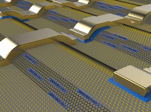
Model of an electronic circuit with electrons (blue) traveling through interconnected graphene nanoribbons (black atoms) grown on steps etched in silicon carbide (yellow atoms) Credit: John Hankinson; Georgia Tech.
Graphene—a single layer of carbon atoms arranged in hexagonal pattern—is like a 2D honeycomb for atom-sized bees. According to a Nature news report, “It is as stiff as diamond and hundreds of times stronger than steel—yet at the same time is extremely flexible, even stretchable. It conducts electricity faster at room temperature than any other known material, and it can convert light of any wavelength into a current.”
I don’t have to highlight all the potential applications of such a material, but it turns out that graphene sounds better on paper than it has been in practice, so far. Its production has proved a challenge, largely owing to expensive and complicated production procedures. Also, potential applications still require some logistical solutions. For example, thin ribbons are ideal for many graphene applications, but previous methods of fabricating ribbons left ragged edges, which disrupt electron flow.
Some of the latest graphene work suggests that scientists may be getting closer to fixing those torn edges. A recent letter published in Nature reports that physicists were able to synthesize graphene nanoribbons from silicon carbide (SiC) wafers. Georgia Institute of Technology, Leibniz Universität Hannover in Germany, Centre National de la Recherche Scientifique in France, and Oak Ridge National Laboratory collaborated on the project. According to the press release from Georgia Tech:
“The nanoribbons are grown epitaxially on silicon carbon wafers into which patterns have been etched using standard microelectronics fabrication techniques. When the wafers are heated to approximately 1,000 degrees Celsius, silicon is preferentially driven off along the edges, forming graphene nanoribbons whose structure is determined by the pattern of the three-dimensional surface. Once grown, the nanoribbons require no further processing.”
In addition to being grown on ridges of silicon carbide, the authors showed that the smooth-edged 40-nm-wide graphene nanoribbons could conduct electricity ten times better than previous theories predicted. Electrons moved through the material so well because they encountered almost no scattering, i.e., ballistic transport. Acording to the paper’s abstract the ballistic conduction mode for these materials is also temperature independent.

Walt de Heer, professor of physics at the Georgia Institute of Technology, poses with equipment used to measure the properties of graphene nanoribbons. Credit: Rob Felt; Georgia Tech.
Walt de Heer (pictured, right), professor of physics and senior author on the study, said in the press release: “This work shows that we can control graphene electrons in very different ways because the properties are really exceptional. This could result in a new class of coherent electronic devices based on room temperature ballistic transport in graphene. Such devices would be very different from what we make today in silicon.”
The paper is “Exceptional ballistic transport in epitaxial graphene nanoribbons” (DOI: 10.1038/nature12952).
A separate Nature Communications report detailed another method for synthesizing graphene nanoribbons, this time from a bottom-up solution-based approach, which would easily allow deposition on Si/SiO2 substrates that could support the thin graphene sheets. The authors produced nanoribbons ~1 nm wide that reached lengths of more than 100 nm, with “atomically smooth armchair edges” and a large electronic bandgap (~1.3 eV). The paper is “Large-scale solution synthesis of narrow graphene nanoribbons” (DOI: 10.1038/ncomms4189).
And even if graphene nanoribbons provide too many fabrication challenges, a group of researchers from Rice Unversity reports in Advanced Functional Materials progress on wet-spun carbon-nanotube fibers to improve future technologies.