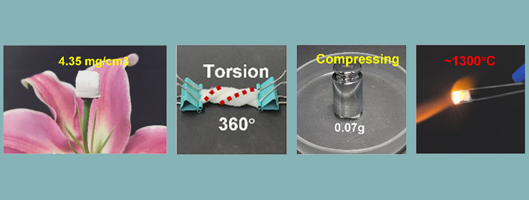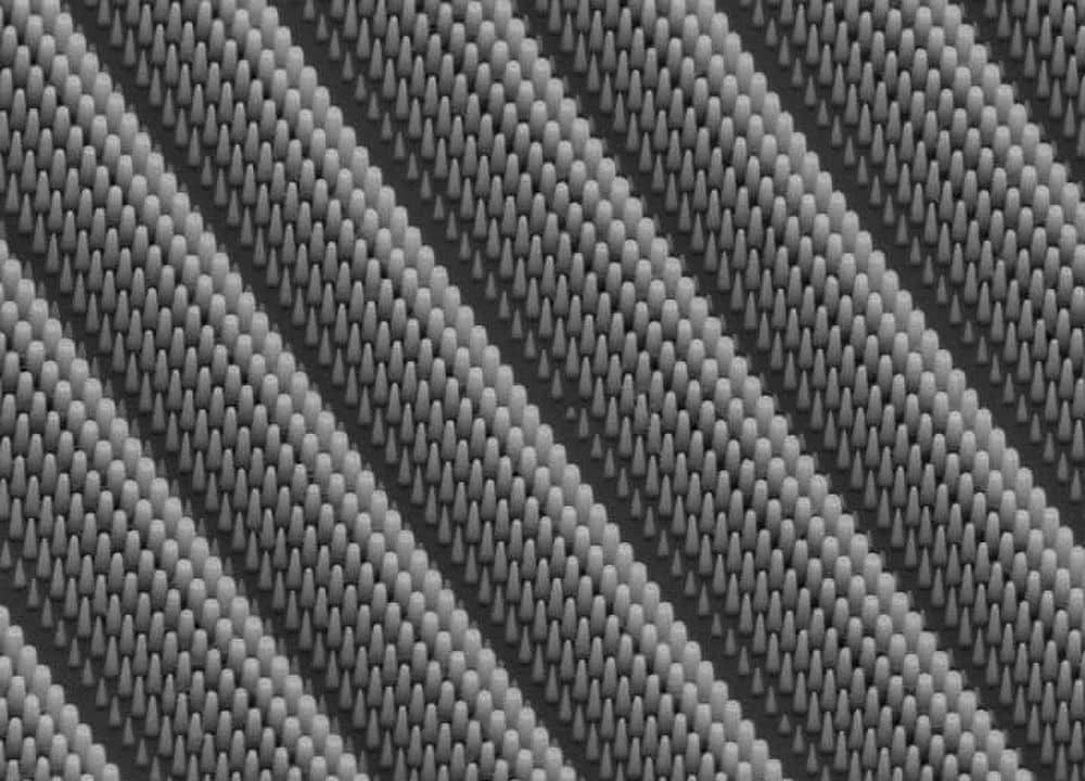
[Image above] Credit: Brookhaven National Laboratory; Flickr CC BY-NC-ND 2.0
Nanotechnology deals with all things science on the nanoscale—that’s on the order of 10–9. Which is why this Sunday, 10/9, is National Nanotechnology Day.
And there’s lots to celebrate—nanotechnology has made a big impact on all forms of science, but in particular materials science. When you go atomically thin, many nanomaterials have vastly different properties than their bulk counterparts, making this field a ripe place for discovery when it comes to both familiar and completely novel materials.
Speaking of small scales, small things are winning big this year—the 2016 Nobel Prize in Chemistry was awarded this week to three chemists— Jean-Pierre Sauvage of France’s University of Strasbourg, J. Fraser Stoddart of Northwestern University in the U.S., and Bernard L. Feringa from the University of Groningen in the Netherlands—for designing and developing atomic-scale molecular machines. What are molecular machines? Watch and learn.
The 2016 Nobel Prize in Physics went to David J. Thouless of the University of Washington, Duncan M. Haldane of Princeton, and J. Michael Kosterlitz of Brown University for their theoretical work to explain strange states of matter. Their work delves into topology, with interesting implications for materials research and more.
But, going back to nanotechnology, here are some of the latest small-scale science discoveries that are sure to make a big impact—although not Nobel Prize big, at least not yet.
Graphene’s defects can be the material’s greatest assets.
Defects in any material can have big effects on its performance—and when those materials are mere atoms thin, defects can drastically change how that material behaves. So doping is an important process when it comes to developing nanomaterials, particularly carbon-based wonder material graphene.
Now a team of scientists at Penn State, Oak Ridge National Lab, and Lockheed Martin Space Systems have devised sophisticated simulations that will allow graphene tinkerers to dope the material to have specific properties.
The scientists used atomistic simulations to accurately predict defects that will form in graphene when the material is doped. This prediction ability provides the tools needed to custom design and fabricate doped graphene with particular properties tailored for a wide range of applications, including membranes for water desalination, energy storage, sensing, or advanced protective coatings.
The paper, published in ACS Nano, is “Atomistic-scale simulations of defect formation in graphene under noble gas ion irradiation” (DOI: 10.1021/acsnano.6b03036).
Defects stack up to strengthen—not weaken—nanomaterials.
Speaking of defects, researchers at Louisiana Tech have similarly found that defects can be the key to strengthening nanomaterials. The Louisiana Tech team used simulations to find that stacked up defects don’t add weakness, but instead strength, to nanomaterials.
The researchers’ simulations show that nanowires with a single stacking fault actually have a higher yield stress than non-defected nanowires—the fault actually makes the material stronger.
That’s because of uneven distribution of stress on the two sides of the defects—opposing compressive and tensile stresses—that affects the material’s mechanical response. And the researchers say the phenomenon is likely occurs in other 1-D materials, too.
For more information, see the Louisiana Tech news release.
Move over graphene—borophene may be better when it comes to flexible electronics.
While graphene has received a substantial proportion of the attention and interest on atomically thin materials, Rice University researchers think that atom-thick boron, called borophene, could have an important edge.
Their work shows that, when grown on a silver substrate, borophene is corrugated, a structure that could make the conductive material ideal for flexible electronics. Although its natural form is flat, simulations show that hexagonal vacancies in borophene help give its its corrugated structure on top of silver.
And because borophene is weakly bound to the silver layer, the researchers suggest that transferring the thin boron layer onto an elastic substrate will keep its wavy surface structure and allow incorporation into flexible electronics.
The paper, published in Nano Letters, is “Substrate-induced nanoscale undulations of borophene on silver” (DOI: 10.1021/acs.nanolett.6b03349).
Fractals may be the key to develop better transparent electrodes.
Researchers at Helmholtz Zentrum Berlin have made observations that suggest that the key to better photovoltaics lies in taking a cue from nature.
Photovoltaics and other technologies have begun to explore the potential of metallic nanowires as conductive elements for transparent electrodes. Those materials are usually arranged in a periodic pattern. But the new research suggests that quasi-fractal nano-features, similar to the hierarchical structure of leaf veins, can improve performance of transparent electrodes.
Fractal-like nano-features optimize performance because they minimize surface coverage and provide low resistance, yet maintain uniform current density. The researchers’ experiments show that their fractally organized metallic mesh offers lower resistance than a periodically-arranged one, boosting output power for photovoltaics and more.
The paper, published in Nature Communications, is “Optimization of hierarchical structure and nanoscale-enabled plasmonic refraction for window electrodes in photovoltaics” (DOI: 10.1038/ncomms12825).
So, in the name of nanotechnology, lace up those sneakers and get going on your 100 billion nanometer dash. And if you want more nano-sized science, check out the American Chemical Society’s special nanotechnology webpage for more on the latest small-scale, big-impact science.
Author
April Gocha
CTT Categories
- Material Innovations
- Nanomaterials
Related Posts
Sports-quality ice: From pond side to precision Olympic engineering
February 12, 2026


