[Image above] Credit: yashima; Flick CC BY-SA 2.0
What do you want for the holidays?
Maybe a ceramic mug that keeps your coffee nice and toasty?
How about some of the world’s smallest—and perhaps cutest—multilayer ceramic capacitors?
Or perhaps you’re jonesing a one-size-fits-all sintering technique that can homogenously densify most all materials in under 30 seconds?
While I can’t vouch for the existence of Santa, or what gifts he might deliver to you, I do know that one-size-fits-all technique is no longer a figment of your materials science imagination.
Researchers at San Diego State University (San Diego, Calif.) have developed a flash spark plasma sintering technique that can densify all kinds of materials, regardless of their electrical conductivity, in a matter of just seconds.
The research builds off the scientists’ previously developed sintering technique, which we reported about on Ceramic Tech Today about a year ago. That flash spark plasma sintering technique, or flash hot pressing, could consolidate silicon carbide powder up to full density in just seconds with the help of a specially designed tooling die. The San Diego State team’s new work is the next step forward for the technique.
That’s important because sintering—a technique integral to materials manufacturing, especially ceramics—is time- and energy-intensive. Redesigned sintering methods that require less energy and less time, and hence reduce manufacturing costs, have been a focus of many research efforts over past several years.
“Our new and rather extraordinary powder consolidation method, in contrast to previous studies, allows extension of flash sintering to nearly all materials and energy-efficient production of small and intermediate size objects with the possibility of complex net-shaping,” Eugene Olevsky, distinguished professor of mechanical engineering and associate dean for research and graduate studies at San Diego State University, explains in an email.
Olevsky along with postdoctoral fellow Charles Manière and Ph.D. student Geuntak Lee designed the sintering technique to create a unique conductive/non-conductive interface that channels electric current in narrowly focused areas in the material being sintered, Olevsky explains.
To do that, the team designed a graphite die sprayed with an electrically insulating layer of boron nitride, which act as conductor and isolator, respectively. Together, this combination concentrates electric current, allowing rapid heating and uniform sintering of various materials.
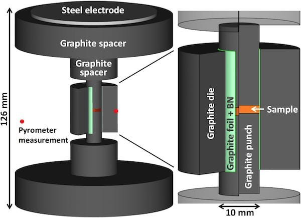
The graphite die setup. Credit: Manière et al.; Scientific Reports
“Highly localized and intensive passage of the electric current is different from regular spark plasma sintering and from previously used schematics of flash spark plasma sintering,” Olevsky says. “In those previously used approaches, the electric current and the Joule heat it generated passed through the whole volume of the graphite tooling and also through the whole volume of the processed powder specimens, if the powder was conductive.”
“In this new approach, electric current is highly concentrated, which makes its impact (heat generation, first of all) highly effective,” Olevsky says.
So effective, in fact, that the team’s new sintering technique can generate densified materials with homogenous microstructures in just 8–35 seconds—whereas conventional sintering techniques can require multiple hours.
And, in addition to fast, the technique is versatile, too. The scientists achieved good sintered densities when they tested the technique on nickel, alumina (Al2O3), and zirconia (3Y-ZrO2) samples.
“Nickel, alumina, and zirconia are not just three randomly chosen materials—they represent electrically conductive (nickel), isolative (alumina), and ionically conductive (zirconia) classes of materials,” Olevsky adds.
“Our experiments showed that all of these material systems can be successfully processed by flash spark plasma sintering with special tooling interface design. This technique turns out to be truly all-materials inclusive—we were able to demonstrate this using these three quite different material systems.”
Olevsky says his team’s findings substantially advance fundamental understanding of field-assisted sintering, taking an important step towards broader industrialization of both flash sintering and spark plasma sintering technologies—which could signify substantial process improvements in manufacturing densified ceramic materials more quickly, with lower energy requirements, and at reduced cost.
The open-access paper, published in Scientific Reports, is “All-materials-inclusive flash spark plasma sintering” (DOI:10.1038/s41598-017-15365-x).
Did you find this article interesting? Subscribe to the Ceramic Tech Today newsletter to continue to read more articles about the latest news in the ceramic and glass industry! Visit this link to get started.