[Image above] Nanowire crystals used as the solar cells. SEM image of GaAs nanowire crystal grown on a silicon substrate. Credit: Krogstrup et al., Niels Bohr Institute.
Nanowire solar cells raise efficiency limit
Scientists from the Nano-Science Center at the Niels Bohr Institute, Denmark, and the Ecole Polytechnique Fédérale de Lausanne, Switzerland, have shown that a single GaAs nanowire can concentrate the sunlight up to 15 times of the normal sun light intensity. These results demonstrate the great potential of development of nanowire-based solar cells, says Peter Krogstrup on the surprising discovery that is described in the journal Nature Photonics. In recent years, the research groups have studied how to develop and improve the quality of the nanowire crystals. It turns out that the nanowires naturally concentrate the sun’s rays into a very small area in the crystal by up to a factor 15. Because the diameter of a nanowire crystal is smaller than the wavelength of the light coming from the sun, it can cause resonances in the intensity of light in and around nanowires. Thus, the resonances can give a concentrated sunlight, where the energy is converted, which can be used to give a higher conversion efficiency. The typical efficiency limit—the so-called “Shockley-Queisser Limit”—is a limit, which for many years has been a landmark for solar cells efficiency among researchers, but now it seems that it may be increased.
Two new joint large-scale research projects at Mainz and Kaiserslautern to supply state-of-the-art technologies to businesses
Two €3.8 million research projects in materials science and spintronics have been initiated at Johannes Gutenberg University Mainz and the University of Kaiserslautern. The two new projects, STeP and TT-DINEMA, are designed to help speed up the process of conversion to marketable procedures and products. The purpose of the Spintronic Technology Platform in Rhineland-Palatinate (STeP) is to promote the sustained build-up of technical competencies and to support regional companies working in the spintronics sector. The platform has been specifically designed to bolster research into and the development of magnetic coating systems, which are particularly suitable for use in products such as sensors and memory storage units. At the core of the research being undertaken by STeP are so-called Heusler materials. The objective is to develop “building block systems” that can then be flexibly adapted to meet the wide range of different functional and technological challenges. The aim of the TT-DINEMA project is to establish an internationally competitive and independent service center that can provide original new material concepts. It represents the starting point for innovative development projects in various fields of applications, ranging from solar technology through medical technology to thermoelectrics, and is likely to be of particular benefit to small and medium-sized companies. Again, Heusler compounds are at the focus of attention concerning the applied materials. In addition to their broad application potential, these materials are also interesting from the commercial point of view because of their low cost, sustainability, environmental friendliness, and ease of processing.
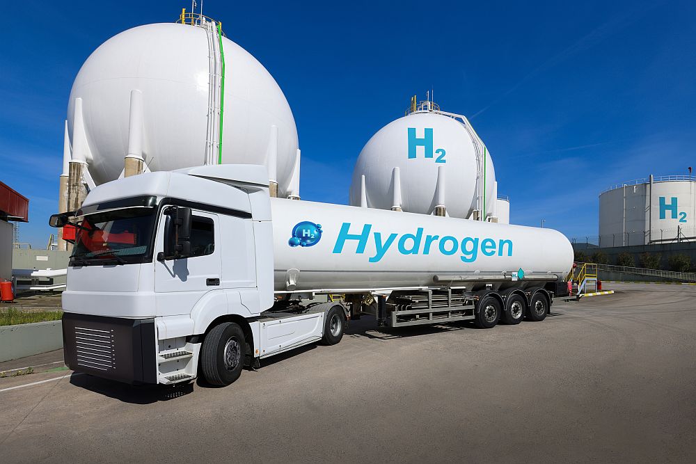
New Sandia book highlights pressing need for hydrogen-powered vehicles
Sandia National Laboratories reveals the breadth of its hydrogen fuel expertise in the recently published Hydrogen Storage Technology—Materials and Applications. Sandia researcher Lennie Klebanoff is confident that the book’s content will give readers a sense of urgency about the need to get zero-emission hydrogen fuel cell vehicles on the road, and to get other hydrogen-based power equipment into the marketplace. Klebanoff, who serves as the book’s editor and cowrote half the chapters, knows his topic well. He was director of the Metal Hydride Center of Excellence, one of three DOE Hydrogen Storage Centers of Excellence dedicated to solving the problem of storing hydrogen on automobiles. This Center, competitively selected and funded through DOE’s Office of Energy Efficiency and Renewable Energy, included 21 partners from industry, academia, and national laboratories from 2005 through 2010. Klebanoff himself said storage isn’t the technical hurdle some believe it to be. “We actually make the argument that storage is not a huge barrier,” he says. “All of the major car manufacturers have produced hydrogen vehicles, and they can all run for at least 240 miles, and in one case, even up to 430 miles.” He acknowledged that the research community must work harder to meet the government and industry consumer vehicle target of at least 300 miles across a range of vehicle types and sizes. “However, there is no technical hydrogen storage barrier preventing the roll-out of the first hydrogen-powered vehicles today,” Klebanoff asserts.
Holes in silicon hold on to their spin
Spintronic devices are almost exclusively fabricated out of n-type semiconductors as opposed to p-type semiconductors, which may seem surprising since both electrons and holes have spin. The reason is that holes have been assumed to be unable to preserve their spin polarization over distances longer than a few tens of nanometers. This perspective is changing, as several recent experiments have shown that hole spins in p-type silicon can be polarized and retain their polarization for a surprisingly long time. However, experiments that directly probe the spin of the holes as they travel through the material have been lacking. Eiji Shikoh at Osaka University, Japan, and colleagues have now performed such an experiment. Writing in Physical Review Letters, Shikoh et al. use a new approach to show that holes in p-type silicon can preserve spin-based information and transport it over distances much longer than previously thought. Taken together, the new work and the previous experiments support the view that spin transport is realistic in p-type semiconductors. This opens the door to developing spintronic devices and circuits that exploit the unique features of p-type semiconductors and their combination with n-type materials.
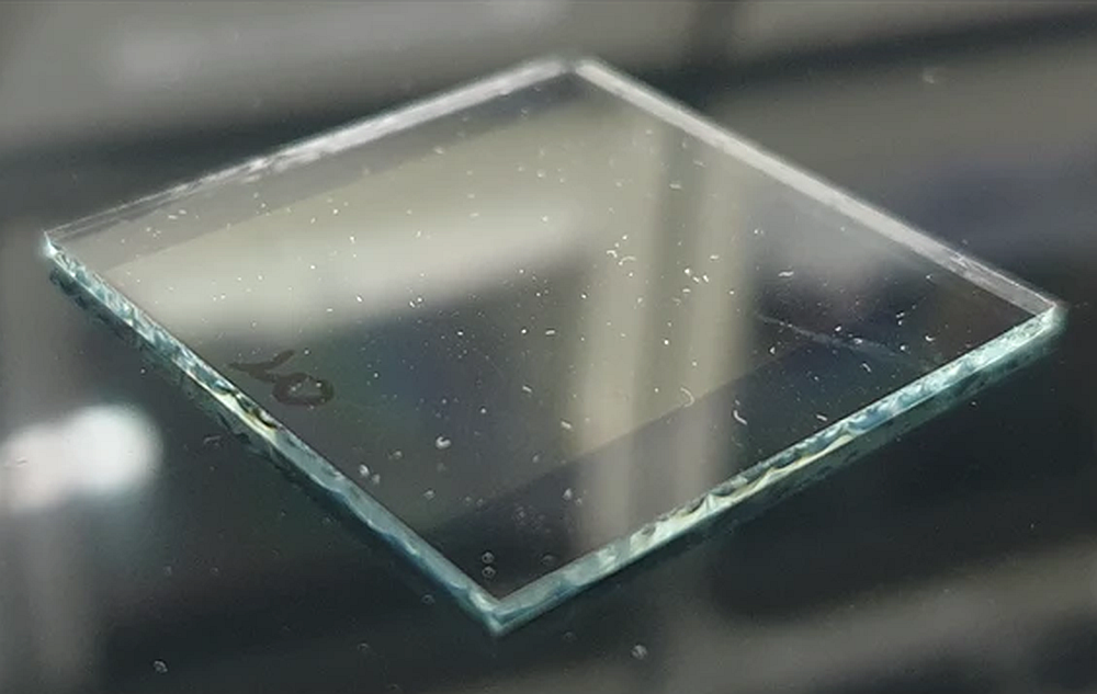
Laser-based glass soldering packages temperature-sensitive glass/glass and glass/ceramics
(Laser Focus World) To package temperature-sensitive glass/glass and glass/ceramics components, especially those with large substrate surfaces to be sealed, a laser-based joining process that uses glass solder is becoming more and more significant. The Fraunhofer Institute for Laser Technology (ILT) is developing the appropriate irradiation strategies and processing heads to achieve this. The advantage of the laser-based joining process is that the laser beam is able to apply energy to a limited space in order to melt the glass solder precisely, thus generating a bond with long-term, stable hermeticity. In laser-based glass soldering, the laser beam is guided over the workpiece and applies the energy solely into the glass solder itself to melt it. One radiation approach for this is quasi-simultaneous laser soldering, but it is technically restricted by the maximum processing field size of the focusing optics, and is also limited, from an economic point of view, by the laser power required. In ILT’s new approach is “contour soldering with energy input adapted laterally to feed movement” that enables large substrates to be joined at significantly lower laser power. For contour soldering, continuous-beam sources run at a power of less than 100 W, independent of the substrate sizes to be joined.
New NIST microscope measures nanomagnet property vital to spintronics
Researchers at NIST have developed a new microscope able to view and measure an important but elusive property of the nanoscale magnets used in an advanced, experimental form of digital memory. The new instrument already has demonstrated its utility with initial results that suggest how to limit power consumption in future computer memories. NIST’s heterodyne magneto-optic microwave microscope, or H-MOMM, can measure collective dynamics of the electrons’ spins-the basic phenomenon behind magnetism-in individual magnets as small as 100 nanometers in diameter. “The measurement technique is entirely novel, the capability that it has enabled is unprecedented, and the scientific results are groundbreaking,” project leader Tom Silva says. As described in a new paper, NIST researchers used the H-MOMM to quantify, for the first time, the spin relaxation process-or damping-in individual nanomagnets. Spin relaxation is related to how much energy is required to switch a unit of spintronic memory between a 0 and a 1. The nanomagnets used in experimental spintronic systems are too big to yield their secrets to conventional atomic physics tools yet too small for techniques used with bulk materials. Until now, researchers have been forced to measure the average damping from groups of nanomagnets. The new microscope enabled NIST researchers to study, in detail, the ups and downs of spin excitation in individual magnets made of a layer of a nickel-iron alloy on a sapphire base.
Have you ever thrown into the fire—even if you shouldn’t have—an empty packet of crisps? The outcome is striking: the plastic shrivels and bends into itself, until it turns into a small crumpled and blackened ball. This phenomenon is explained by the tendency of materials to pick up their original features in the presence of the right stimulus. Hence, this usually happens when heating materials that were originally shaped at high temperatures and cooled afterwards. EPFL researchers realized that this phenomenon occurred to ultrathin quartz tubes (capillary tubes) under the beam of a scanning electron microscope. “This is not the original microscope’s purpose. The temperature increase is explained by an accumulation of electrons in the glass. Electrons accumulate because glass is a non-conductive material,” explains Lorentz Steinbock, researcher at the Laboratory of Nanoscale Biology and co-author of a paper on this subject published in Nano Letters. As the glass shrinks, it can be seen live on the microscope screen. “It’s like a glass-blower. Thanks to the possibilities provided by the new microscope at EPFL’s Center of Micronanotechnology, the operator can adjust the microscope’s voltage and electric field strength while observing the tube’s reaction. Thus, the person operating the microscope can very precisely control the shape he wants to give to the glass”, says Aleksandra Radenovic, tenure-track assistant professor in charge of the laboratory. At the end of this process, the capillary tube’s ends are perfectly controllable in diameter, ranging from 200 nanometers to fully closed.