MIT researchers improve efficiency of quantum-dot photovoltaic system by adding a forest of nanowires
Photovoltaics based on tiny colloidal quantum dots have several potential advantages over other approaches to making solar cells. But there’s a tradeoff in designing such devices because of two contradictory needs for an effective PV: A solar cell’s absorbing layer needs to be thin to allow charges to pass readily from the sites where solar energy is absorbed to the wires that carry current away—but it also needs to be thick enough to absorb light efficiently. Improved performance in one of these areas tends to worsen the other, says Joel Jean, a doctoral student in MIT’s Department of Electrical Engineering and Computer Science. The addition of zinc oxide nanowires can play a useful role, says Jean, who is the lead author of a paper to be published in the journal Advanced Materials. These nanowires are conductive enough to extract charges easily, but long enough to provide the depth needed for light absorption, Jean says. Using a bottom-up growth process to grow these nanowires and infiltrating them with lead-sulfide quantum dots produces a 50 percent boost in the current generated by the solar cell, and a 35 percent increase in overall efficiency, Jean says. The process produces a vertical array of these nanowires, which are transparent to visible light, interspersed with quantum dots.
Nanotubes boost potential of salinity power as a renewable energy source
(Gizmag) In November 2009, Norwegian state owned electricity company Statkraft opened the world’s first osmotic power plant prototype, which generates electricity from the difference in the salt concentration between river water and sea water. While osmotic power is a clean, renewable energy source, its commercial use has been limited due to the low generating capacities offered by current technology – the Statkraft plant, for example, has a capacity of about 4 kW. Now esearchers have discovered a new way to harness osmotic power that they claim would enable a 1 square meter (10.7 sq. ft.) membrane to have the same 4 kW capacity as the entire Statkraft plant. The global osmotic, or salinity gradient, power capacity, which is concentrated at the mouths of rivers, is estimated by Statkraft to be in the region of 1,600 to 1,700 TWh annually. Electricity can be generated through the osmotic phenomena that results when a reservoir of fresh water is brought into contact with a reservoir of salt water through the use of a special kind of semipermeable membrane in one of two ways—either by harnessing the osmotic pressure differential between the two reservoirs to drive a turbine, or by using a membrane that only allows the passage of ions to produce an electric current.
Don’t call it vaporware: Scientists use cloud of atoms as optical memory device
(NIST Tech Beat) Talk about storing data in the cloud. Scientists at the Joint Quantum Institute (JQI) of the NIST and the University of Maryland have taken this to a whole new level by demonstrating that they can store visual images within quite an ethereal memory device—a thin vapor of rubidium atoms. The effort may prove helpful in creating memory for quantum computers. Their work builds on an approach developed at the Australian National University, where scientists showed that a rubidium vapor could be manipulated in interesting ways using magnetic fields and lasers. The vapor is contained in a small tube and magnetized, and a laser pulse made up of multiple light frequencies is fired through the tube. The energy level of each rubidium atom changes depending on which frequency strikes it, and these changes within the vapor become a sort of fingerprint of the pulse’s characteristics. If the field’s orientation is flipped, a second pulse fired through the vapor takes on the exact characteristics of the first pulse-in essence, a readout of the fingerprint.
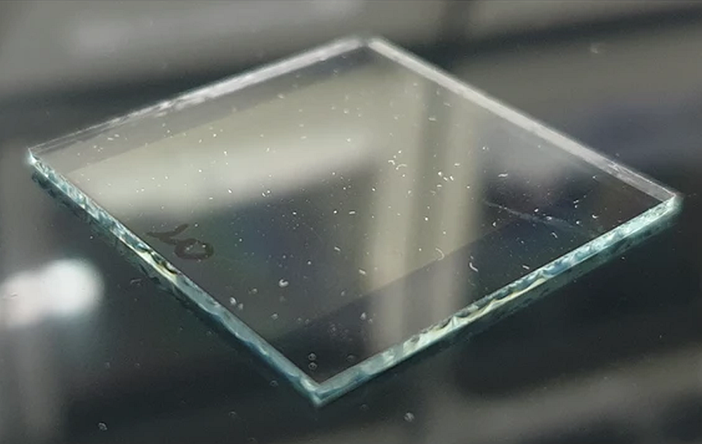
Recyclable solar cells made from trees
Fabricating new plant-based solar cells on cellulose nanocrystal substrates means that they’re recyclable in water. Researchers report that the organic solar cells reach a power conversion efficiency of 2.7 percent, an unprecedented figure for cells on substrates derived from renewable raw materials. The cellulose nanocrystal (CNC) substrates on which the solar cells are fabricated are optically transparent, which lets light pass through them before being absorbed by a very thin layer of an organic semiconductor. During the recycling process, the solar cells are simply immersed in water at room temperature. Within minutes, the CNC substrate dissolves and the solar cell can be separated easily into its major components. To date, organic solar cells have been typically fabricated on glass or plastic. Neither is easily recyclable, and petroleum-based substrates are not very eco-friendly. For instance, if cells fabricated on glass were to break during manufacturing or installation, the useless materials would be difficult to dispose of. “Our next steps will be to work toward improving the power conversion efficiency over 10 percent, levels similar to solar cells fabricated on glass or petroleum-based substrates,” says Bernard Kippelen, a professor at the Georgia Institute of Technology’s College of Engineering, who led the study. The group plans to achieve this by optimizing the optical properties of the solar cell’s electrode.
A step toward optical transistors?
As demand for computing and communication capacity surges, the global communication infrastructure struggles to keep pace, since the light signals transmitted through fiber-optic lines must still be processed electronically, creating a bottleneck in telecommunications networks. While the idea of developing an optical transistor to get around this problem is alluring to scientists and engineers, it has also remained an elusive vision, despite years of experiments with various approaches. Now, McGill University researchers have taken a significant, early step toward this goal by showing a new way to control light in the semiconductor nanocrystals known as “quantum dots.” In results published online recently, researchers show that all-optical modulation and basic Boolean logic functionality—key steps in the processing and generation of signals—can be achieved by using laser-pulse inputs to manipulate the quantum mechanical state of a semiconductor nanocrystal. Quantum dots already are used in applications ranging from photovoltaics, to light-emitting diodes and lasers, to biological imaging. Patanjali (Pat) Kambhampati’s McGill group’s, latest findings point toward an important new area of potential impact, based on the ability of these nanocrystals to modulate light in an optical gating scheme. “These results demonstrate the proof of the concept,” Kambhampati says. “Now we are working to extend these results to integrated devices, and to generate more complex gates in hopes of making a true optical transistor.”
Nanotechnology imaging breakthrough
A team of researchers has made a major breakthrough in measuring the structure of nanomaterials under extremely high pressures. For the first time, they developed a way to get around the severe distortions of high-energy X-ray beams that are used to image the structure of a gold nanocrystal. The technique, described in Nature Communications, could lead to advancements of new nanomaterials created under high pressures and a greater understanding of what is happening in planetary interiors. Lead author of the study, Wenge Yang of the Carnegie Institution’s High Pressure Synergetic Consortium explains, “The only way to see what happens to such samples when under pressure is to use high-energy X-rays produced by synchrotron sources. Synchrotrons can provide highly coherent X-rays for advanced 3D imaging with tens of nanometers of resolution. This is different from incoherent X-ray imaging used for medical examination that has micron spatial resolution. The high pressures fundamentally change many properties of the material.” The team found that by averaging the patterns of the bent waves-the diffraction patterns-of the same crystal using different sample alignments in the instrumentation, and by using an algorithm developed by researchers at the London Centre for Nanotechnology, they can compensate for the distortion and improve spatial resolution by two orders of magnitude.
Author
Eileen De Guire
CTT Categories
- Basic Science
- Electronics
- Energy
- Optics