[Image above] A game of networking bingo helped break the ice for attendees at the Student and Young Professionals Mixer on Thursday evening. Credit: ACerS
As the winter chill faded, Denver, Colo., basked in beautiful weather, setting the stage for the highly anticipated Electronic Materials and Applications (EMA) Conference, which took place Feb. 25–28, 2025.
EMA is coorganized by ACerS Basic Science and Electronics Divisions. For EMA 2025, Basic Science Division organizers were Fei Peng of Clemson University and Ming Tang of Rice University. Electronics Division organizers were Mina Yoon of Oak Ridge National Laboratory and Reeja Jayan of Carnegie Mellon University.
This year’s conference marked a significant milestone as the largest EMA gathering to date, welcoming more than 400 attendees from 17 countries. Additionally, the event’s prime location near the Colorado School of Mines facilitated the participation of more than 100 students.
“This year’s EMA was a great success: a vibrant gathering that brought together a diverse mix of attendees, from energetic graduate students to seasoned professionals with decades of experience,” says organizer Mina Yoon. “The high quality of presentations and lively discussions, all focused on the electronic and fundamental science perspectives of ceramics research, truly embodied the spirit of our well-established community.”
ACerS Director of Meetings Andrea Ross also expressed immense satisfaction with the turnout, noting there were many new faces in the crowd this year.
“We have great momentum as we head into next year’s ACerS Spring Meeting, where our Basic Science and Electronics Divisions will program, along with our Bioceramics, Energy Materials and Systems, Glass and Optical Materials, and Manufacturing Divisions,” she says.
Highlights from EMA 2025 are below.
Plenary lectures: Advancing materials design with machine learning
EMA 2025 attendees had the privilege of engaging with two insightful plenary lectures on Wednesday and Thursday mornings. These lectures highlighted the integration of data science, specifically machine learning, in materials design.
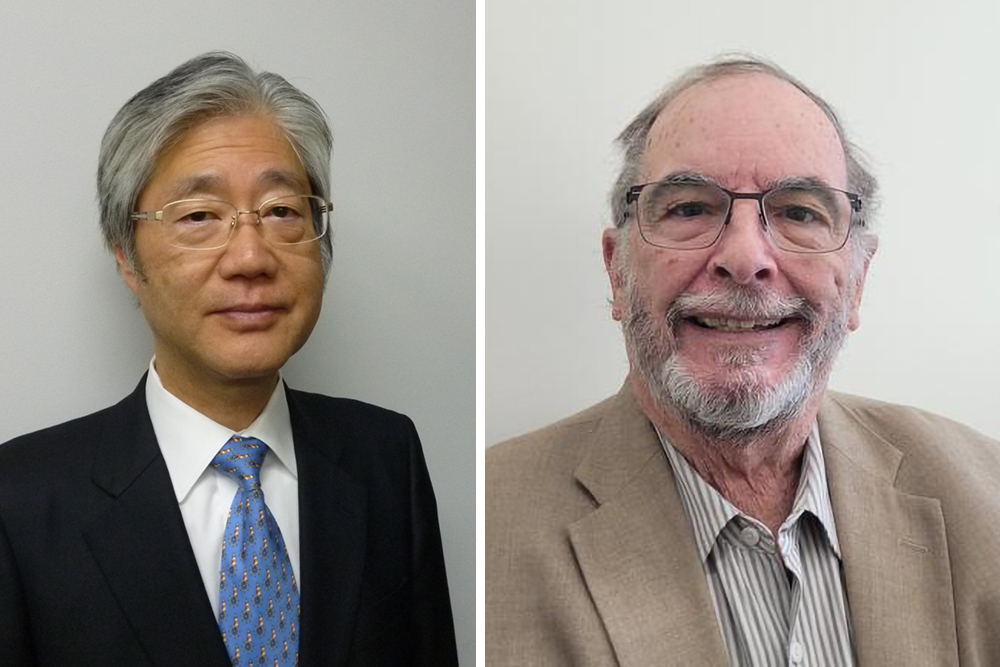
Jian Luo of the University of California, San Diego delivered the first plenary lecture, which overviewed his team’s work on developing grain boundary phase diagrams, “arguably the most useful materials science tool” for understanding material behavior at the atomic level. Luo described how they used a combination of thermodynamic models, atomistic simulations, and machine learning to develop the diagrams, and then showed how they aided in the investigation of electric field-induced grain boundary phase transitions.
Sergei Kalinin of the University of Tennessee, Knoxville delivered the second plenary lecture, which highlighted the emerging field of machine learning-assisted materials design. He described how his team has used machine learning techniques to optimize synthesis and characterization workflows. Specifically, by introducing a reward function concept, Kalinin showed how his team successfully bridged the gap between experimental processes and real-world applications, ultimately enhancing the throughput of material discoveries.
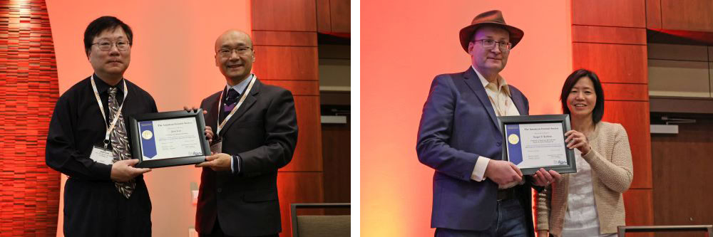
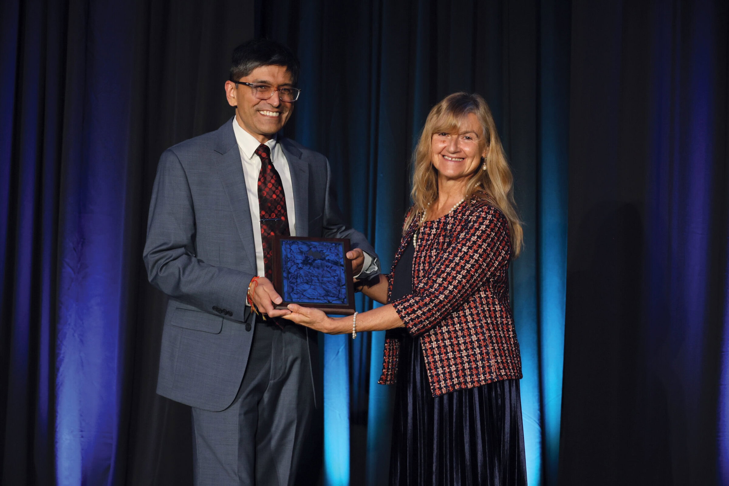
EMA 2025 organizers Fei Peng (Basic Science Division) and Mina Yoon (Electronics Division), right in each photo, presented their Division’s respective plenary lecturers, Jian Luo and Sergei Kalinin, with certificates of appreciation following their talks on Wednesday and Thursday mornings. Credit: ACerS
Tutorials and receptions empower student participation at EMA
One of the highlights of EMA 2025 was the remarkable level of student participation, with students making up more than 25% of the total attendees. Several special events at EMA 2025 helped empower this participation.
First, two student-focused tutorials took place on Tuesday and Wednesday evenings. The first tutorial, organized by the Basic Science Division, explored machine learning in materials science, and it drew wide interest from both students and professionals. The second tutorial, organized by the Electronics Division, discussed electron ptychography of ceramic materials. While the Basic Science tutorial is a long-standing event, this year was the first time the Electronics Division held a tutorial, and attendees welcomed this addition to the programming.
A Student and Young Professionals Mixer also took place on Thursday evening. More than 100 attendees attended the event and engaged in networking bingo, which allowed them to foster valuable connections with their peers and seasoned colleagues.
The conference ended on Friday with the ever-popular “Failure: The Greatest Teacher” symposium, where established researchers share stories about experiments that did not work out to show students that failure is a natural part of doing science. This year, Katherine Page shared her personal experience with failures in a presentation titled “Craze-y Ruddlesden-Popper complex ceramics.”
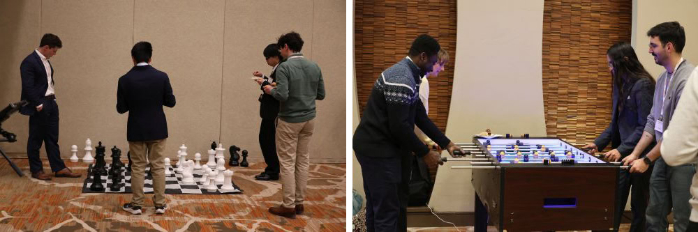
Attendees enjoyed games of giant chess, foosball, and air hockey during the Celebration of EMA reception on Thursday evening. Credit: ACerS
A new chapter: ACerS Spring Meeting 2026
Next year, the Basic Science and Electronics Divisions will come together with the Bioceramics, Energy Materials and Systems, Glass & Optical Materials, and Manufacturing Divisions at the new ACerS Spring Meeting, which will take place April 12–16, 2026, in Bellevue, Wash. This expanded event welcoming six ACerS Divisions will create more opportunities for cross-disciplinary collaborations.
“EMA as a standalone event will be missed, but we look forward to our next meeting in a new setting as we continue to grow and strengthen our community!” says organizer Mina Yoon.
View more images from EMA 2025 on ACerS Flickr page.