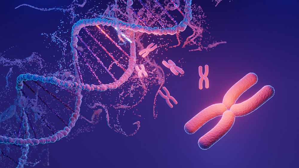
[Image above] 3D rendering of DNA, which has a double helix shape (shown in upper left). DNA makes up the thread-like strands called chromosomes (the X-shaped structure shown bottom right). Rearrangement of DNA within the chromosome can cause different genetic diseases. Credit: tanatpon13p, Shutterstock
In the past decade, at-home genetic testing has become a huge market, enticing consumers with the novelty of learning about their heritage. I did one as well to learn about my ancestors! (Turns out I’m mostly German, English, and Swedish, with some other regions sprinkled in.)
But the advancements that have taken place in genetic testing since 2000 enable much more than mapping family trees. They also greatly improve the ability to diagnose DNA translocations, which can be a key indicator of certain genetic diseases, such as various cancers.
A DNA translocation involves a chromosome breaking off (typically into two pieces), with the broken pieces attaching to different chromosomes. In some cases, pieces from two different chromosomes trade places with each other.
There are several genetic and molecular techniques used to diagnose translocations, including
- Karyotypics, which analyzes the structure of chromosomes using a laboratory-produced image of a person’s chromosomes. (The chromosomes are isolated from an individual cell and arranged in numerical order.)
- Fluorescence in situ hybridization, which uses fluorescent probes to identify specific chromosomal regions.
- Next-generation sequencing techniques, which can rapidly sequence millions of DNA or RNA fragments simultaneously.
Among the different types of next-generation sequencing techniques, nanopore sequencing is commonly used to diagnose translocations. This technique involves threading a DNA strand through a nanopore, creating tiny electrical signals that are detected and converted to read each base.*
*NOTE: A DNA base is a nitrogen-containing molecule. There are four primary bases (adenine, cytosine, guanine, and thymine) forming specific pairs, each carrying genetic information.
Commercially available nanopore sequencing technologies use naturally occurring nanopores in biological materials. However, researchers are investigating engineering nanopores in solid-state materials because these materials offer several advantages.
Notably, various solid-state materials are compatible with wafer-scale manufacturing processes and so can be integrated with local electronic sensors. As a result, researchers could achieve massively parallelized, low-cost sequencing of DNA with solid-state nanopores in contrast to biological nanopores.
However, integrating solid-state nanopores with sensors remains challenging due to the extremely small scale required for potential sensors. Currently, successful implementations of this technology are limited to in-plane architectures, such as tunneling junctions and transistors.
Furthermore, the ultrathin 3D materials traditionally used in these devices can have rough surfaces. If dangling bonds (i.e., unpaired valence electrons) are present in the rough surface, it can impact electrical performance, which hinders detection of translocation.
Due to these complications, “There had been a pause on the idea of solid-state DNA transistors for a decade or so,” says Sihan Chen, postdoctoral researcher at the University of Illinois Urbana-Champaign (UIUC), in a UIUC press release.
Shen is part of a team led by two UIUC researchers who aimed to reinvigorate research in this area by taking advantage of their different expertise. Arend van der Zande, associate professor of mechanical science and engineering and materials science and engineering, is an expert in the field of 2D materials, and Rashid Bashir, professor of bioengineering and dean of The Grainger College of Engineering, is an expert in the field of nanopore sensors.
The two UIUC researchers and their colleagues investigated the 2D materials molybdenum disulfide and tungsten diselenide as solid-state materials for nanopores because these materials, like other 2D materials, naturally exist as monolayers with no dangling bonds. They were used to form a vertically stacked 2D heterojunction, which was integrated into a nanopore membrane to create a nanometer-thick, out-of-plane diode through which the molecule passes.
Vertical 2D junctions have an atomically sharp energy band discontinuity at their heterointerface, with the conducting layers separated by only an angstrom-sized van der Waals gap. These properties make diodes incorporating this structure ideal candidates for use as electrical sensing membranes.
The membrane stack was fabricated using the following steps:
- Hafnium oxide membranes, which are hydrophilic and durable in salt solutions, are formed by atomic layer deposition.
- Molybdenum disulfide and tungsten diselenide flakes are transferred onto the membrane to form a 2- to 5-nm thick layer.
- n-type and p-type ohmic contacts to the molybdenum disulfide and tungsten diselenide layer are fabricated using evaporated nickel/gold contacts and transferred gold contacts.
- A multilayer hexagonal boron nitride flake is transferred onto the molybdenum disulfide and tungsten diselenide layer to fully encapsulate the heterostructure. This encapsulation layer enhances the heterostructure’s chemical and mechanical stability and durability while preserving the spatial resolution of the atomically sharp 2D heterointerface for sensing.
- To provide electrical insulation and stable operation, another layer of hafnium oxide is deposited.
- A nanopore is drilled in the overlap region through the membrane stack using a focused electron beam in scanning transmission electron microscopy mode to minimize electron-beam-induced damage.
The resulting solid-state nanopore heterostructure not only measured the changes in electrical current through the diode during DNA translocation, but it also enabled concurrent control of the DNA translocation speed through the application of out-of-plane biases across the diode.
Notably, these results were achieved using both ionic and diode currents, and the researchers demonstrated a 2.3-fold electrostatic slowing of average translocation speed. (A slower translocation speed enables higher temporal resolution.)
These results highlight the potential of solid-state nanopores for “sensitive single-biomolecule analysis with high spatial resolution and extended interrogation time,” the researchers write. However, to experimentally confirm this potential will require a one to two orders of magnitude improvement in both signal-to-noise ratio and dwell time.
“In the future, we envision arrays of millions of 2D diodes with nanopores inside that could read out the sequences of DNA in parallel, reducing sequencing time from two weeks to as little as one hour,” Bashir says in the press release. Furthermore, the price of sequencing could potentially be reduced tenfold compared to current methods.
The researchers write that future work may include “exploring band-to-band tunneling with type-III band alignment and measuring correlated intralayer currents within each semiconductor layer to complement interlayer measurement.”
They may also investigate adding a voltage source between the reference electrode in the electrolyte solution and the diode. This addition would allow independent control of the source and drain sides of the diode relative to the solution, leading to enhanced control of DNA translocation.
The paper, published in Proceedings of the National Academy of Sciences, is “Detecting DNA translocation through a nanopore using a van der Waals heterojunction diode” (DOI: 10.1073/pnas.2422135122).
Author
Laurel Sheppard
CTT Categories
- Biomaterials & Medical
- Nanomaterials


