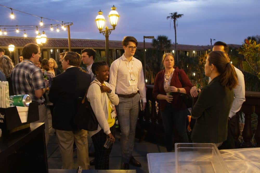
[Image above] Students and young professionals gather for an outdoor reception at EMA 2023. This year is the first time attendees were able to meet in person since 2020 due to the COVID-19 pandemic. Credit: ACerS
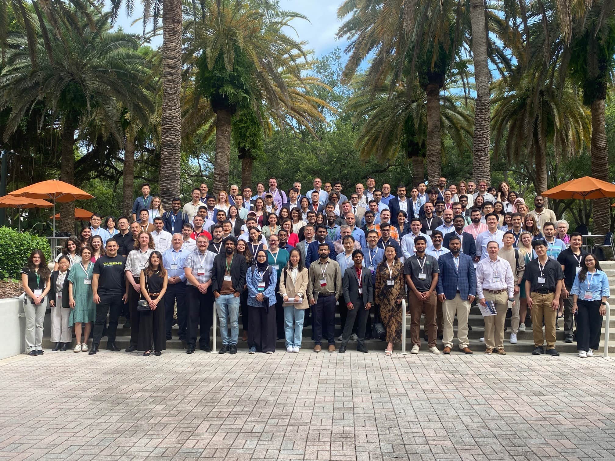
Florida’s January weather can be fickle, either glorious or blustery. Fortunately, the weather in Orlando was glorious and perfect for the Electronic Materials and Applications Conference on Jan. 17–20, 2023.
This conference is coorganized by ACerS’ Electronics Division and Basic Science Division. This year is the first time attendees were able to meet in person since 2020 due to the COVID-19 pandemic, which forced organizers to present EMA in virtual format in 2021 and 2022. While organizers and speakers did a great job creating an EMA virtual experience, all agreed that attending in person provided far better opportunities for discussion and interaction.
For EMA 2023, Electronics Division organizers were Edward Gorzkowski (Naval Research Laboratory) and Matjaz Spreitzer (Josef Stefan Institute, Slovenia). Basic Science Division organizers were Amanda Krause (Carnegie Mellon University) and Ricardo Castro (University of California, Davis).
Close to 270 attendees from 20 countries attended the three-day conference. Below are some highlights from the event.
EMA offers first professional conference experience for many students
Of the 40 students at EMA 2023, for many of them, this meeting was their first time attending a professional conference. The pandemic robbed many graduate students of the opportunity to present their work and get feedback. For example, I met one first-time student who will defend her Ph.D. this spring!
The conference experience is critically important for students, who gain valuable feedback on their work during discussions in the technical sessions. But, more importantly, conferences help students meet prospective employers and collaborators, as well as provide an environment for students to network with each other and build their own professional communities.
A student and young professional reception, poster session, student poster and presentation awards, and a lunch-and-learn career panel discussion were all designed to accelerate student engagement and access to everything the conference had to offer.

Material structure–property relationships the focus of this year’s plenary lectures
The conference opened both of its full-day sessions with a plenary lecture.
The first plenary lecture was presented by Andriy Zakutayev from the National Renewable Energy Laboratory in Golden, Colo. He talked about the discovery and design of electronic materials using high-throughput experimental methods, focusing specifically on ferroelectric materials for energy technologies and computing (transistors and capacitors).
“Energy-efficient computing is an important and ripe problem for materials design and discovery,” he says.
Lead zirconate titanate (PZT) is a well-established material, but it can be tricky to integrate with silicon chips, according to Zakutayev. Using high-throughput methods, his group looked at nitride ferroelectric materials, beginning with wurtzite-structured (Al,Sc)N. The material is easier to integrate with silicon and gallium nitride chips, but it is more difficult (i.e., less efficient) to switch.
This drawback led the team to ask whether there are other polar nitride structures besides wurtzite that could be candidate replacements for PZT. Nitrides derived from wurtzite and rock-salt structures can be integrated with each other, which would allow combinations with halides, such as aluminum nitride, copper iodide, copper bromide, and copper chloride. However, the breakdown field becomes an issue with the introduction of halides.
In the absence of suitable wurtzite nitride compositions, new polar nitride materials—such as perovskite-structure LaWN3, CeWN3, and CeMoN3—merit investigation. These materials may have interesting magnetic properties, too, opening the prospect of next-generation multiferroic materials.

Lehigh University professor and ACerS Fellow Jeffrey Rickman delivered the Day 2 plenary lecture on interfacial phase transitions at grain boundaries and their impact on thermal and mechanical properties.
Through close analysis of grain boundary structures, Rickman and his colleagues came to understand that grain boundaries undergo transitions similar to bulk phase transitions. These grain boundary transitions are called complexions to distinguish from bulk phases. Complexions present in various structures—such as clean, monolayer, bilayer, and trilayer—and transition diagrams, similar to phase diagrams, can be constructed.
Why do complexions matter? Grain boundaries tend to be thought of as the “weak link” in the macroscopic properties of components. But grain boundary complexions are “a big disruption to the bulk,” according to Rickman. In other words, grain boundary structure influences structure and properties of the bulk grains.
For example, abnormal grain growth in the bulk is a lagging signal of complexion transitions due to changes in mobility at the grain boundary. Other properties tied to complexion transitions include rapid vs. slow oxidation, brittle vs. ductile behavior, high vs. low ionic conductivity, and thermal conductivity.
What can we learn about the thermodynamics and kinetics of complexion transitions, and what does that knowledge give us in terms of tools for engineering grain boundaries?
Rickman used silicon carbide to illustrate that complexion transitions can alter material properties, specifically thermal conductivity.
To explore the thermodynamics and kinetics of complexion transitions, Rickman used doped alumina to show that grain boundary complexions modify interfacial modes. This finding led to the question of whether complexions can modify thermal transport. Rickman then successfully showed that complexion structure can be tuned using temperature and chemical potential, and that a lag time can be established between complexion transitions and abnormal grain growth.
Though not simple, complexions can be described thermodynamically, giving researchers new tools in their quiver for understanding and engineering grain boundary structure and properties—and the structure and properties of the bulk.

As delightful as Florida was this year, it also marked the end of an era. Electronics Division and Basic Science Division leaders announced at the conference’s reception that the meeting will move next year to Denver, Colo., and will be held Feb. 13–16, 2024. Without question, the Rocky Mountains will provide a spectacular backdrop. Mark your calendars now for EMA 2024!
Check out all the images from EMA 2023 on ACerS Flickr page.