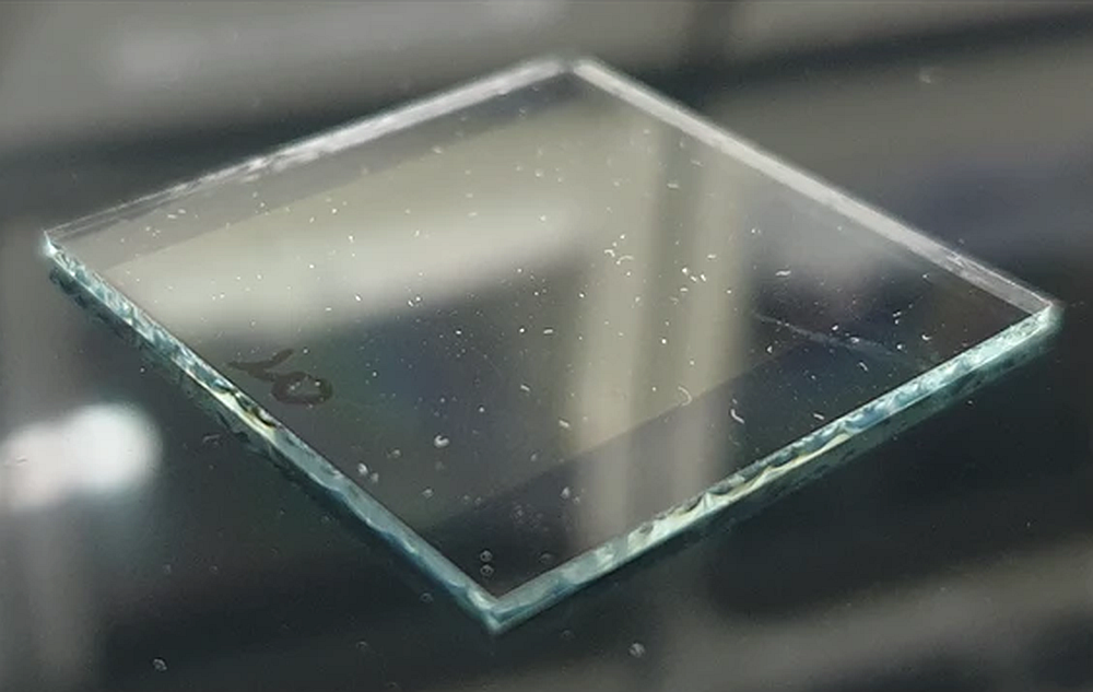
[Image above] This 3D image of a ceramic composite specimen imaged under load at 1,750°C shows the detailed fracture patterns that LBNL researchers are able to view using ALS Beamline 8.3.2. The vertical white lines are the individual silicon carbide fibers in this sample about 500 microns in diameter. Credit: LBNL.
When you have some extra time, check these developments out:
ALS ceramics materials research advances engine performance
LBNL senior materials scientist and UC Berkeley professor Rob Ritchie has been researching the fracture behavior of a wide array of materials for the past 40 years, the last ten of them using the facilities at the ALS. From human bone to synthetic engineering materials such as shape-memory metals and composites, Ritchie has illuminated groundbreaking cracking patterns and the underlying mechanistic processes using the x-ray synchrotron micro-tomography at ALS Beamline 8.3.2. One of Ritchie’s latest materials research projects is contributing to the evolution of jet engine performance, and hence has industry players heavily interested and invested. Termed ceramic-matrix composites, the materials that Ritchie, specifically with his postdoc Hrishikesh Bale, are now studying can withstand temperatures that would melt current state-of-the-art engine material, alloy-based nickel.Ritchie and his group are currently probing the depths of ceramics composites’ fracture and temperature resistance at beam line 8.3.2 as part of a collaborative research project with Teledyne, funded by NASA and the Air Force. Ritchie’s team has developed a unique facility that permits mechanical testing of these composites at very high temperatures with simultaneous real-time 3D imaging of materials. The inherent brittleness of ceramics has been overcome in the new composite materials by creating hybrid microstructures.
Cambridge researchers develop printable lasers
A way of printing lasers using everyday inkjet technology has been created by University of Cambridge scientists. The development has a wide range of possible applications, ranging from biomedical testing to laser arrays for displays. Today, most lasers are made on silicon wafers using expensive processes similar to those used to make microprocessors. However, scientists have now designed a process to “print” a type of organic laser on any surface, using technology very similar to that used in the home. The process involves developing lasers based on chiral nematic liquid crystals, similar to the materials used in flat-panel LCD displays. These are a unique class of photonic materials that, under the right conditions, can be stimulated to produce laser emissions. If aligned properly, the helix-shaped structure of the LC molecules can act as an optically resonant cavity—an essential component of any laser. After adding a fluorescent dye, the cavity can then be optically excited to produce laser light. Researchers from the Centre for Molecular Materials for Photonics and Electronics and the Inkjet Research Centre—both in the Department of Engineering—have devised a way to align the LC molecules and produce high resolution multicolor laser arrays in one step, by printing them. Using a custom inkjet printing system, the researchers printed hundreds of small dots of LC materials on to a substrate covered with a wet polymer solution layer. As the polymer solution dries, the chemical interaction and mechanical stress cause the LC molecules to align and turn the printed dots into individual lasers.
Video reveals molecule ‘gridlock’ in glass
Physicists have made a movie of particle motion as a super-cooled liquid approaches the glass state-a first look at the molecular level of this mysterious process. Their findings, showing how the rotation of the particles becomes decoupled from their movement through space, appear in the Proceedings of the National Academy of the Sciences. “Cooling a glass from a liquid into a highly viscous state fundamentally changes the nature of particle diffusion,” says Emory University physicist Eric Weeks, whose lab conducted the research. “We have provided the first direct observation of how the particles move and tumble through space during this transition, a key piece to a major puzzle in condensed matter physics.”
Shooting electrons at a cloaking device (or other metamaterial) gets it to glow
(Ars Technica) The big problem with measuring how light travels through a photonic crystal is getting light into the crystal. In fact, the better the photonic crystal is, the harder it is to get light into it. To get light into the photonic crystal, you need to choose the right color, polarization, and direction of travel; the light entering the photonic crystal has to be in one of the modes of the photonic crystal. Those can only be discovered through measurements. In other words, to measure the optical behavior of a photonic crystal you need to get some light into it, and you can’t get light into the photonic crystal without knowing its optical behavior. The crudest approach is to simply bounce light off the top of the photonic crystal. None of the light can get into the modes of the crystal, but it can penetrate a little way into the crystal and then reflect. The alternative is to place fluorescent dyes in the photonic crystal. When they are excited, the colors and direction in which the light is emitted forms a map of the modes of the photonic crystal-though only over the limited range of colors that the dye can emit. This sounds awesome, but the presence of the dye changes the very modes you are trying to measure. The presence of the materials in the photonic crystal make it more likely that the dye will choose to get rid of its energy through generating heat instead of light? These uncertainties make the measurements very difficult to interpret. A new paper in Nature solves these problems very cleverly. Essentially, they shoot electrons at the photonic crystal. As the electrons travel down a hole in the crystal, the electrons in the surrounding material are driven away from the edges of the hole. Then once the electron has passed, they come swinging back, pulled in by the excess of positive charge. Of course, they over-shoot, so the swinging carries on for a little while, but is quickly damped out.
Penn Researchers Find New Way to Prevent Cracking in Nanoparticle Films
Making uniform coatings is a common engineering challenge, and, when working at the nanoscale, even the tiniest cracks or defects can be a big problem. New research from University of Pennsylvania engineers has shown a new way of avoiding such cracks when depositing thin films of nanoparticles. To generate a nanoparticle film, the desired particles are suspended in a suitable liquid, which is then thinly and evenly spread over the surface through a variety of physical methods. The liquid is then allowed to evaporate, but, as it dries, the film can crack like mud in the sun. “One method for preventing cracking is modifying the suspension’s chemistry by putting binding additives in there,” says Penn graduate student Jacob Prosser. “But that is essentially adding a new material to the film, which may ruin its properties.” This dilemma is highlighted in the case of electrodes, the contact points in many electrical devices that transfer electricity. High-end devices, like certain types of solar cells, have electrodes composed of nanoparticle films that conduct electrons, but cracks in the films act as insulators. Adding a binder to the films would only compound the problem. One reason this approach may have remained untried is that it is counterintuitive that it should work at all. The method the researchers used to make the films is known as “spin-coating.” A precise amount of the nanoparticle suspension—in this case, silica spheres in water—is spread over the target surface. The surface is then rapidly spun, causing centrifugal acceleration to thin the suspension over the surface in a uniform layer. The suspension then dries with continued rotation, causing the water to evaporate and leaving the silica spheres behind in a compacted arrangement.
Fraunhofer researchers make solar cells made from black silicon
Solar cells convert three-quarters of the energy contained in the Sun‘s spectrum into electricity—yet the infrared spectrum is entirely lost in standard solar cells. In contrast, black silicon solar cells are specifically designed to absorb this part of the sun‘s spectrum—and researchers have recently succeeded in doubling their overall efficiency. The sun blazes down from a deep blue sky – and rooftop solar cells convert this solar energy into electricity. Not all of it, however: Around a quarter of the sun’s spectrum is made up of infrared radiation which cannot be converted by standard solar cells – so this heat radiation is lost. One way to overcome this is to use black silicon, a material that absorbs nearly all of the sunlight that hits it, including infrared radiation, and converts it into electricity. But, how is this material produced? “Black silicon is produced by irradiating standard silicon with femtosecond laser pulses under a sulfur containing atmosphere,” explains Stefan Kontermann, who heads the research group, “Nanomaterials for Energy Conversion,” within the Fraunhofer Project Group for Fiber Optical Sensor Systems at the Fraunhofer Institute for Telecommunications, Heinrich-Hertz-Institut. “This structures the surface and integrates sulfur atoms into the silicon lattice, making the treated material appear black.” If manufacturers were to equip their solar cells with this black silicon, it would significantly boost the cells’ efficiency by enabling them to utilize the full Sun spectrum. Researchers at HHI have now managed to double the efficiency of black silicon solar cells—in other words, they have created cells that can produce more electricity from the infrared spectrum. “We achieved that by modifying the shape of the laser pulse we use to irradiate the silicon,” says Kontermann.
University of Buffalo partners with Zimbabwe universities to create nanotechnology center
With 14 percent of Zimbabwe’s population living with HIV/AIDS and tuberculosis as a co-infection, the need for new drugs and new formulations of available treatments is crucial. To address these issues, two of UB’s leading research centers-the Institute for Lasers, Photonics and Biophotonics and the New York State Center of Excellence in Bioinformatics and Life Sciences-have signed on to launch the Zimbabwe International Nanotechnology Center, a national nanotechnology research program, with the University of Zimbabwe and the Chinhoyi University of Technology. This collaborative program initially will focus on research in nanomedicine and biosensors at UZ and energy at CUT. ZINC has grown out of the NIH Fogarty International Center’s AIDS International Training and Research Program that was awarded to UB and UZ in 2008 to conduct HIV research training and build research capacity in Zimbabwe and neighboring countries in southern Africa. ZINC will establish a long-term international research and training platform in the field of nanotechnology focused in areas that promote Zimbabwe’s strength and advance the development of nanotechnology as an avenue for the country’s commercial growth.