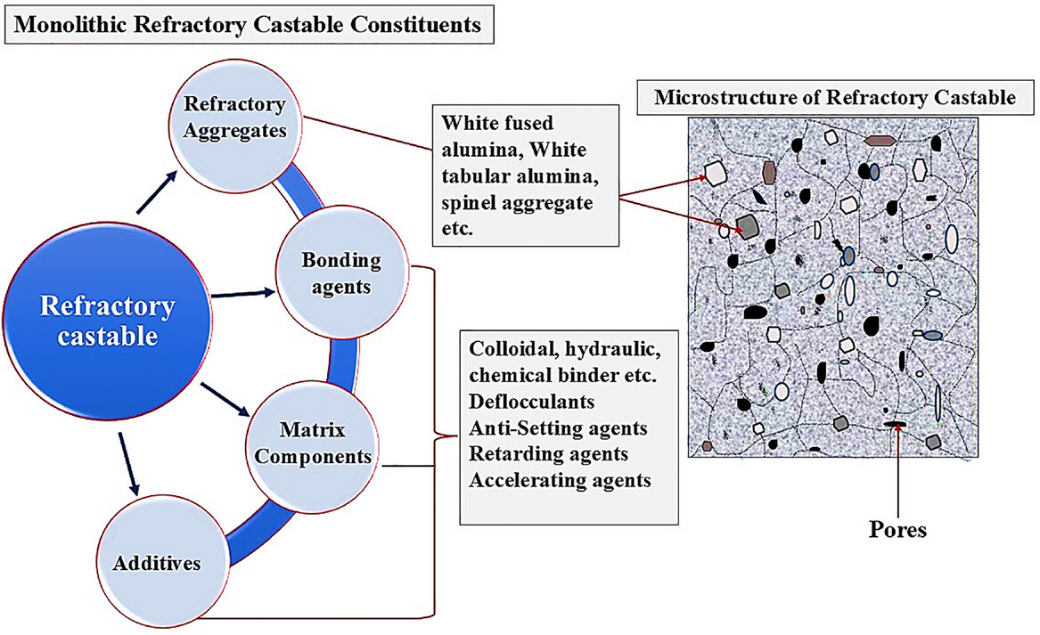
[Image above] Associate Professor Michael Arnold (left) and graduate student Gerald Brady and their team made carbon nanotube transistors that, for the first time, surpass state-of-the-art silicon transistors, thus achieving a big milestone in nanotechnology. Credit: Stephanie Precourt
Electronic devices are facing a revolution—and that revolution wouldn’t be possible without harnessing the power of advanced materials.
Obvious standout materials like graphene and silicon have ruled the research buzz when it comes to faster, flexible, durable electronics. Although these materials are superstars on their own, they’re even more impressive when they team up with would-be formidable opponents.
For example, in July, researchers at the University of California, Riverside, and the University of Georgia (Athens, Ga.) integrated graphene with 2-D nanomaterials to reshape next-gen consumer electronics. And, earlier this year, researchers at the University of Oxford in England found that perovskites paired with silicon could create higher-efficiency solar cells.
However, when it comes to high-performance transistors, silicon’s been the go-to material. Recently, though, researchers at the University of Wisconsin-Madison say carbon nanotube transistors have, for the first time, outperformed silicon.
Led by Michael Arnold and Padma Gopalan, UW-Madison professors of materials science and engineering, the team’s carbon nanotube transistors achieved current that’s 1.9 times higher than silicon transistors, according to a university press release.
“This achievement has been a dream of nanotechnology for the last 20 years,” says Arnold. “Making carbon nanotube transistors that are better than silicon transistors is a big milestone. This breakthrough in carbon nanotube transistor performance is a critical advance toward exploiting carbon nanotubes in logic, high-speed communications, and other semiconductor electronics technologies.”
The mission to harness the unique properties of carbon nanotubes for use in high-performance electronics is decades-long, but numerous challenges have caused their development to fall behind semiconductors such as silicon and gallium arsenide.
“Carbon nanotube transistors should be able to perform five times faster or use five times less energy than silicon transistors, according to extrapolations from single nanotube measurements. The nanotube’s ultra-small dimension makes it possible to rapidly change a current signal traveling across it, which could lead to substantial gains in the bandwidth of wireless communications devices,” according to the release.

The team used a solution process to deposit aligned arrays of carbon nanotubes onto 1 inch by 1 inch substrates. The scalable and rapid deposition process coats the entire surface of this substrate with aligned carbon nanotubes in less than five minutes. Credit: Stephanie Precourt
Challenge number one: The struggle is real when isolating purely carbon nanotubes. And that’s a crucial step because “metallic nanotube impurities act like copper wires and disrupt their semiconducting properties, like a short in an electronic device,” the release explains.
So the team achieved a solution of ultra-high-purity semiconducting carbon nanotubes by using polymers to sort out the semiconducting nanotubes.
“We’ve identified specific conditions in which you can get rid of nearly all metallic nanotubes, where we have less than 0.01 percent metallic nanotubes,” says Arnold.
Challenge number two: Controlling placement and alignment of the nanotubes isn’t easy.
“To make a good transistor, the nanotubes need to be aligned in just the right order, with just the right spacing, when assembled on a wafer,” the release explains. The researchers devised a solution to this problem in 2014 with a technique called “floating evaporative self-assembly,” that gives them this control.
Challenge number three: Good electrical contact between the nanotubes and the metal electrodes of the transistor is crucial.
The polymer the team used to isolate the semiconducting nanotubes creates an insulating layer between the nanotubes and the electrodes. To eliminate this barrier, the team “baked” the nanotube arrays in a vacuum oven to remove the insulating layer, which resulted in excellent electrical contacts to the nanotubes.
Going a step further, the researchers also developed a treatment that removes residues from the nanotubes after they’re processed in solution.
“In our research, we’ve shown that we can simultaneously overcome all of these challenges of working with nanotubes, and that has allowed us to create these groundbreaking carbon nanotube transistors that surpass silicon and gallium arsenide transistors,” says Arnold.
This advance could pave the way for carbon nanotube transistors to replace silicon transistors, particularly in wireless communications technologies that require a lot of current flowing across a small area.
“There has been a lot of hype about carbon nanotubes that hasn’t been realized, and that has kind of soured many people’s outlook,” says Arnold. “But we think the hype is deserved. It has just taken decades of work for the materials science to catch up and allow us to effectively harness these materials.”
The research, published in Science Advances, is “Quasi-ballistic carbon nanotube array transistors with current density exceeding Si and GaAs” (DOI: 10.1126/sciadv.1601240).