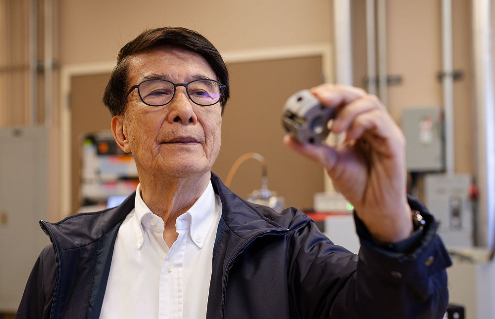
[Image above] Credit: Marco Cologna & Rishi Raj, University of Colorado.
Words such as “novel” and “revolutionary” get thrown around fairly frequently in science and engineering circles, but the still-young technique of flash sintering, in theory, could deliver a broad revolution in the preparation of ceramic materials, and it appears it will soon be put to a significant manufacturing test by a UK-based company, Ceram.
If you haven’t heard of flash sintering before, you are certainly not alone. Aside from a (growing) body of papers in ACerS’ journals (as well a few other peer-reviewed materials journals), posts in this blog and a feature story in this month’s ACerS’ Bulletin, not a lot has been written as yet in the broad scientific and engineering media about flash sintering. I am not sure why that is. Perhaps it is because sintering and kiln technology have an old fashion ring to them and do not carry the high-tech cachet that accompanies novel electronics, biomedical, energy and defense-oriented glass and ceramic research.
But, I would argue that flash sintering—if it continues to pan out as it is scaled up—could be one of the most profound and disrupting developments in materials in the last 50 years (if not millennia, given how long mankind has been trying to fire ceramic objects or melt glass), at least from an energy-consumption point of view. And, if you have ever seen even modern, relatively energy-efficient ceramic production lines (making, for example, tiles, whiteware, refractory brick, construction brick, etc.), you know the current process still requires long heating (sometime over a day) and the use of energy-intensive tunnel or massive box kilns.
But flash sintering may change nearly all of that.
For the sake of simplicity, you can think of flash sintering as a traditional sintering/kiln process, but with special twist: The heating takes place in the presence of an electrical field. Surprisingly, because of the effects of the electrical field, as the ceramic object reaches a critical (and relatively low) temperature, it suddenly sinters in a few seconds rather than hours and hours. There is a lot of research and speculation about the exact mechanisms that allow flash sintering to occur, but part of the phenomenon likely has to do with the electrical field allowing the ceramic grains to align and slide past each other. A defect avalanche mechanism might also enhance diffusion. Oddly, there is also a photoemission effect that has been detected, which seems to also signify that the formation of electron hole pairs plays of role.
Regardless of the mechanism, the good news is that flash sintering has been tested many times on relatively small scales and appears to work on nearly every type of ceramic material. (It also seems to be an effective way to rapidly melt glass—but that’s a story for another day.)
Despite a lot of initial (and not inappropriate) leeriness and “too good to be true” thinking when reports of flash sintering first appeared, the caution has evolved into general enthusiasm among ceramic scientists and engineers, and some of that enthusiasm has started to spill over into the manufacturing community. That is because the potential energy and CO2 emissions savings from flash sintering in the ceramics and glass sectors is staggering.
Regarding manufacturing, when I interviewed University of Colorado’s Rishi Raj for my Bulletin story, he mentioned that he is working to scale-up the technology with Ceram, a subsidiary of British Ceramics Research and a well known international company focused on materials testing, analysis and consultancy. Raj predicted that a place to start introducing flash sintering into the business side of things might be to develop a new kiln system for ceramic tile manufacturing, where energy costs are high and business competition is intense. He mentioned that one challenge would be developing a non-contact electrode system to provide the electrical field.
The non-contact electrode challenge must have been solved because the project with Ceram now appears to have started. A few days ago, the Westland (UK) version of TheBusinessDesk.com reported that at Ceram, “Work has started on a kiln that is to be the basis for technology that could cut energy costs for ceramics firms by up to 30 percent.”
The same story says Ceram is calling the effort the Low Energy Firing Project and describes it as an “80-feet-long commercial-scale kiln.” It also reports that construction of the new kiln is supposed to be completed this month, and testing is to begin in May. It goes on to say, “[T]he first commercial-scale results should be available before the end of the year.”
The story intriguingly quotes David Pearmain, the LEFP project manager, who says, “The potential of this work is really exciting. We think we can reduce firing times as well as temperatures, so there could be very, very significant advantages for the sector.”
I am curious how Ceram came up with its projected 30 percent savings figure, and I suspect that is on the conservative side. I have reached out to officials at Ceram for more details on the LEFP and hope to have more details next week.
Author
Eileen De Guire
CTT Categories
- Basic Science
- Energy
- Manufacturing


