[Image above] Close-up of a silicon die being extracted from the semiconductor wafer and attached to the substrate. Credit: IM Imagery, Shutterstock
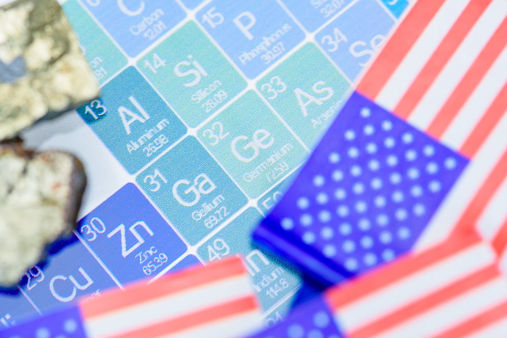
In the four decades since a toaster was first connected to the internet, there are now more than 18 billion connected Internet of Things devices around the world. With billions more expected to be added by the end of this decade, it is crucial that new and improved semiconductor technologies be developed to handle the growing demands on data storage, transport, and processing infrastructure.
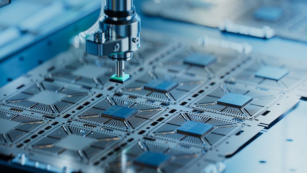
Governments around the world have dedicated more funding to semiconductor manufacturing, and universities are following their lead by launching new laboratories and institutes focused on semiconductor research and development. Below is an overview of some of the facilities announced since the beginning of 2025.
Prototyping and advanced packaging piloting facility at ASU
On January 6, Arizona State University announced that it had been selected by the U.S. Commerce Department and Natcast as the site of the co-located NSTC Prototyping and NAPMP Advanced Packaging Piloting Facility. The facility will combine semiconductor research and prototyping for front-end manufacturing and packaging capabilities. It is expected to be operational as early as the fourth quarter of 2028. Learn more.
Semiconductor thin film laboratory at Penn State
On February 26, The Pennsylvania State University announced plans to establish an advanced laboratory for semiconductor thin films and device research in the Materials Research Institute’s facilities in the Millennium Science Complex at University Park. At the heart of the new facility, made possible by funding from regional microelectronics consortium MMEC, will be a metal-organic chemical vapor deposition tool. Learn more.
Nanofabrication Lab at Nevada
On April 8, the University of Nevada, Reno announced the grand opening of the Nanofabrication Lab in the Davidson Foundation Cleanroom in the William N. Pennington Engineering Building. The facility is equipped with tools for lithography, deposition, etching, wire bonding, and metrology, which can be used to manufacture electronic, photonic, and quantum devices. Learn more.
MUT–Imperial SABER Lab at Imperial College London
On June 6, Imperial College London announced the opening of the MUT–Imperial Semiconductor AI & BioSensor Electronics Research Lab (SABER Lab). The facility, opened in collaboration with Mahanakorn University of Technology, will bring together Imperial’s expertise in integrated circuit design and biomedical electronics and MUT’s state-of-the-art training facilities and electronics design. Learn more.
TSMC–UTokyo Lab at the University of Tokyo
On June 12, the University of Tokyo and Taiwan Semiconductor Manufacturing Company announced the opening of the TSMC-UTokyo Lab, which is dedicated to advancing semiconductor research, education, and talent incubation. This facility builds on a collaboration between the two organizations that has been ongoing since 2019. Learn more.
Newly merged research institute at TU/e
On June 19, Eindhoven University of Technology announced it is establishing a research institute dedicated to semiconductors, quantum, photonics, and the development of high-tech systems and chips of the future. The new institute merges one existing institute with two initiatives: the Eindhoven Hendrik Casimir Institute, the High Tech Systems Center, and the Future Chips Flagship. The official launch of the new institute will take place at the end of September 2025. Learn more.
Semiconductor research and development facility at Stony Brook University
On July 17, New York State Governor Kathy Hochul announced that Stony Brook University and onsemi, the largest U.S.-based manufacturer of silicon carbide power semiconductors, will construct a $20 million, state-of-the-art semiconductor research and development facility on the Stony Brook University campus. Research at the new center will aim to unlock the full potential of silicon carbide chips. The center is expected to be fully operational in early 2027. Learn more.
MOCVD Laboratory at UW-Madison
On August 5, the University of Wisconsin-Madison’s Ultrawide Bandgap Semiconductor Metal-Organic Chemical Vapor Deposition Laboratory officially opened. The facility will serve as the cornerstone of the College of Engineering-led focus on III-nitride semiconductors, which can handle much higher voltages than silicon-based semiconductors. Learn more.