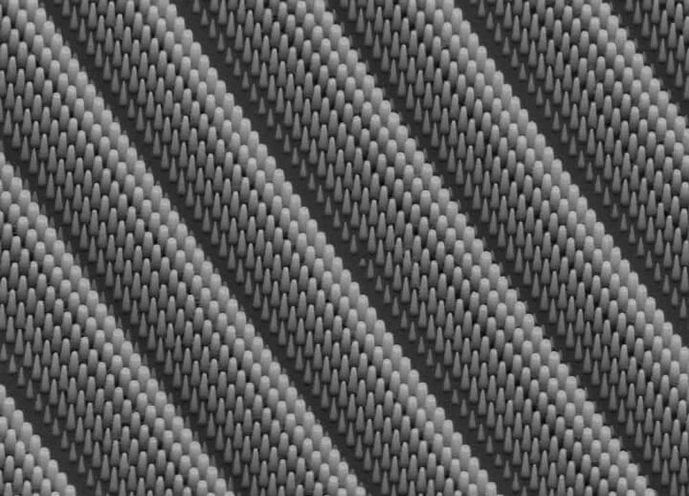
[Image above] A multiwall carbon nanotube with triple-wall, “arm chair” morphology. Global production capacity of MWNTs is about 4.5 kilotons per year. Credit: Eric Weiser; Wikimedia.
Twenty years is the figure cited in Materials Genome Initiative presentations and documents as the typical time span between new material discovery and commercialization. The MGI aspires to reduce the timeline by half to 10 years.
Carbon nanotubes seem to be a good example of a new material that transitioned from discovery to commercialization quickly. CNTs today are used in applications as disparate as Tour de France bicycle frames, antifouling paints, microelectronic interconnects, supercapacitors, water filters, wind turbine blades, nonvolatile random access memory devices, and more. A review article in the Feb. 1, 2013, issue of Science (subscription required) highlights applications for multiwall and single-wall CNTs (MWNT and SWNT, respectively). It also describes manufacturing-scale synthesis and processing methods, economic challenges, and overall outlook for CNT commercialization.
According to the article, worldwide CNT production increased by more than a factor of 10 between 2006 and 2011. In 2005, the year that a CNT composite bicycle won the Tour de France, annual global production capacity hovered around 0.2 kilotons. By 2011, global CNT production capacity soared to about 4.6 kilotons per year. (The authors observe that a plethora of press releases promote new applications, but are skimpy on technical details. Production capacity provides a clue to the trajectory of commercialization success.)
(Note: I could not confirm that the 2005 Tour de France winning bike was a CNT composite. Its rider was Lance Armstrong.)
The article reports that most CNTs produced today are disorganized (unaligned), which limits the ability to capitalize on the interesting properties of aligned structures such as yarns, “forests,” and sheets. Nevertheless, there are enough applications for CNTs incorporated into bulk composites and thin films that the authors say CNT powders are “now entering the growth phase of their product life cycle.”
Chemical vapor deposition is the prevailing manufacturing-scale method for synthesizing in production quantities of MWNTs. SWNTs require much closer control of the CVD process, which keeps their prices much higher than MWNTs (by orders of magnitude, according to the article). However, CNTs can still be pricey, themselves (and the reason your touring bike is not a CNT composite)—up to about $100 per kilogram, which is as much as 10 times the price of carbon fiber.
The article provides a brief overview of applications of CNTs in composite materials, coatings and films, microelectronics, energy storage and environment, and biotechnology.
As CNTs progress through their life cycles, manufacturers (and those that regulate their activities) will have to address health and safety standards, disposal and recycling of discards, environmental impact, etc.
In addition addressing the producibility of SWNTs, the graphene family of nanoscale carbon materials shows promise for commercial applications ranging from thermal interfaces to aerogel coatings to corrosion prevention coatings. Lessons learned during the transition of CNT technology out of the lab and into the production line should pay dividends for commercializing graphene.
So, what about that timeline from discovery to commercialization?
Pinpointing the discovery of CNTs is not so easy. In 1991 Japanese physicist, Sumio Iijima, published a paper on CNTs that seems to have been the spark that ignited subsequent intense research and development efforts. Iijima is often credited with being the inventor of CNTs. However, this Wikipedia article (which seems to have done a thorough job tracing the big history of the tiny tubes) traces the 40-year history of CNTs prior to 1991!
The first published report of CNTs was in 1952 in a Soviet-era, Russian language journal, and therefore, not noticed. A 1976 article demonstrated vapor phase growth of single wall carbon nanotubes. Other early reports were published in 1979 and 1981. In 1987 the USPTO issued a patent for the production of “Cylindrically discrete carbon fibrils” with diameters between 3.5 and 70 nanometers.
Arguably, in 1952 the characterization tools, like transmission electron microscopes, were either rudimentary or did not exist. Probably the same for production processes, like CVD. Consider, too, that even the applications did not exist. The first demonstration of the solid-state transistor, for example, only happened in 1947. The point is that the finish line may be easier to define than the starting point. It seems to me that MGI goals should be careful not to dismiss novel materials as “failures” even if commercialization takes more than 20 years.
Author
Eileen De Guire
CTT Categories
- Electronics
- Energy
- Manufacturing
- Nanomaterials


