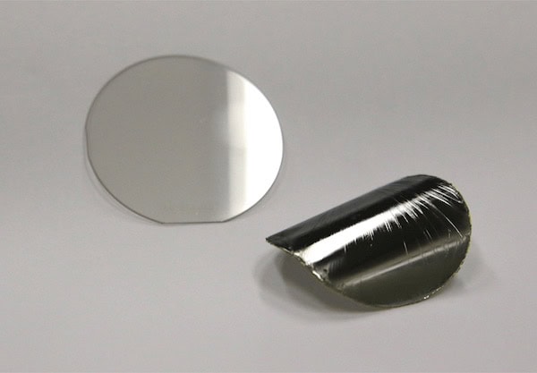
[Image above] A thick bulk gallium nitride crystal wafer (2 in. in diameter) with a gallium nitride thin film—~20 microns thick, or 1/5th the thickness of a sheet of paper—fabricated by controlled spalling in the foreground. Credit: Bedell; IBM Research
A couple of years ago, I wrote about how gallium nitride was tousling with silicon for a prime position reigning over the electronics world.
Like all epic battles, it seems that the fight continues.
Gallium nitride, a material already used in LED lights and high-power electronics, is so promising because of the material’s excellent electronic, optoelectronic, and tribological properties.
Plus, gallium nitride could enable all new kinds of devices like bendable LEDs and more powerful power packs—and to do so, the material seems to be taking a very thin page from graphene’s book.
IBM scientists report that they have developed a simple technique to peel extremely thin layers of gallium nitride from a bulk wafer of the material—a breakthrough in manufacturing techniques for this expensive material.
In addition to the added benefits of being lightweight and flexible, thin layers are advantageous because they mean that more material can be generated from a single wafer, a key to reducing manufacturing costs.
Plus, thin layers of gallium nitride have lower electrical resistance and can dissipate heat more easily, which means that thin films boast enhanced performance, too.
“Our approach to thin film removal is intriguing because it’s based on fracture,” Stephen W. Bedell, research staff member at IBM Research and one of the paper’s authors, says in an AIP news release. “First, we deposit a nickel layer onto the surface of the material we want to remove. This nickel layer is under tensile strength—think drumhead. Then we simply roll a layer of tape onto the nickel, hold the substrate down so it can’t move, and then peel the tape off. When we do this, the stressed nickel layer creates a crack in the underlying material that goes down into the substrate and then travels parallel to the surface.”
Using tape to isolate extremely thin layers from bulk material is no breakthrough—scientists have previously devised simple “Scotch tape methods” to peel off atomically thin layers of graphene from graphite, although such DIY methods produce small and sometimes inconsistent flakes of thin material.
But the IBM Research method, called controlled spalling, produces thin layers without crystalline damage to the material. The researchers report in the paper’s abstract that, using transmission electron microscopy, they couldn’t even detect defects in the thin films they generated.

The flexibility of a 20-micron-thick film. Credit: Bedell; IBM Research
The team originally described its controlled spalling technique back in 2013 and has already used the technique to successfully fabricate thin layers of silicon, germanium, gallium arsenide, gallium nitride/sapphire, and amorphous materials.
And because the technique is performed at room temperature and “can be applied at nearly any time in the fabrication flow, from starting materials to partially or fully finished circuits,” Bedell says in the release, it’s significant for the semiconductor industry.
Plus, adjusting the thickness of the nickel layer controls how much of the surface peels off, allowing the researchers to tune the thickness of thin layers.
“The basic mechanism of substrate spalling fracture started out as a materials science problem,” Bedell says. “It was known that metallic film deposition would often lead to cracking of the underlying substrate, which is considered a bad thing. But we found that this was a metastable phenomenon, meaning that we could deposit a thick enough layer to crack the substrate, but thin enough so that it didn’t crack on its own—it just needed a crack to get started.”
Creating that seed crack is easy, the scientists say—simply end the nickel layer abruptly near the edge.
“This creates a large stress discontinuity at the edge of the nickel film so that once the tape is applied, a small pull on the tape consistently initiates the crack in that region,” Bedell adds in the release.
The team is reportedly now collaborating with partners to use the spalling technique to fabricate high-voltage gallium nitride devices.
The paper, published in the Journal of Applied Physics, is “Layer transfer of bulk gallium nitride by controlled spalling” (DOI: 10.1063/1.4986646).
Author
April Gocha
CTT Categories
- Electronics
- Manufacturing
- Nanomaterials
- Thermal management


