The time-to-market gap for commercially viable graphene just keeps shrinking, with promising new developments every day that aim to manufacture graphene to produce faster, higher-performing, more efficient electronics and other applications.
Thanks to graphene’s single-layer thickness, toughness, and supreme mechanical and thermal properties, the material is an ideal choice for developing electronic, optoelectronic, and electromechanical devices and sensors.
Graphene has historically been an expensive, labor-intensive material to produce for commercial applications—but scientists are pioneering innovative solutions for producing this high-potential material in a way that’s scalable.
And they continue to make strides in the mission to commercialize graphene so the advanced material can be put to work in real-world ways.
Check out these three graphene-related research developments generating buzz this week.
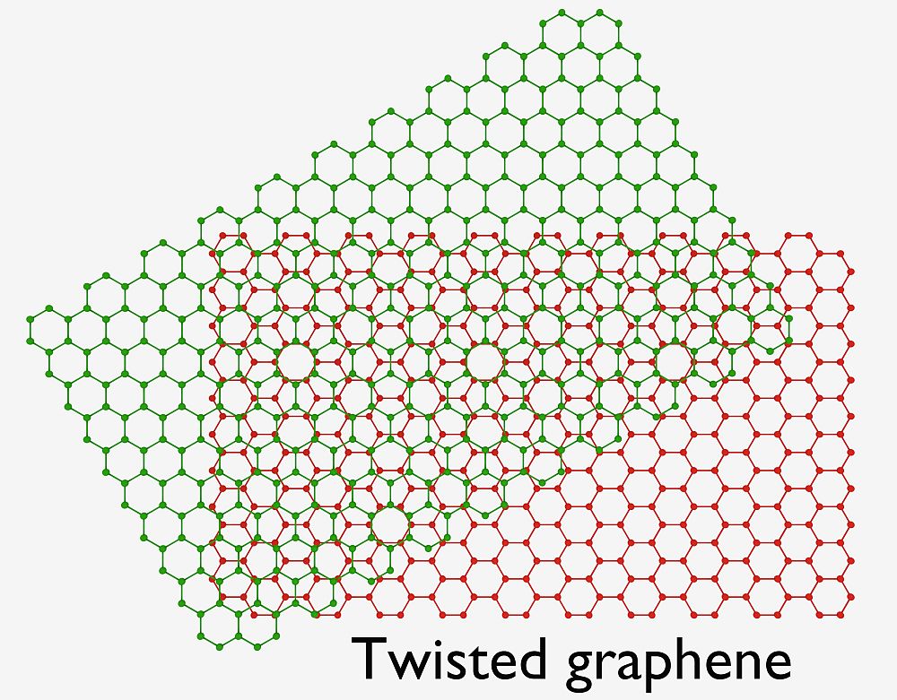
Graphene goes highly crystallized for better stability.
Researchers at Osaka University in Japan have discovered a procedure that restores defective graphene oxide structures that cause the material to display low carrier mobility.
“By applying a high-temperature reduction treatment in an ethanol environment, defective structures were restored, leading to the formation of a highly crystalline graphene film with excellent band-like transport,” according to a university press release. The researchers say these findings could pave the way for more scalable production techniques of highly crystalline graphene films.
Novel bi-layer graphene device that “controls electrons” could revolutionize next-gen electronics.
A team of Penn State University scientists (State College, Pa.) developed a device made of bilayer graphene with the ability to control the momentum of electrons that offers a path to electronics that could require less energy and give off less heat than standard silicon-based transistors.
“Current silicon-based transistor devices rely on the charge of electrons to turn the device on or off, but many labs are looking at new ways to manipulate electrons based on other variables, called degrees of freedom,” Jun Zhu, associate professor of physics at Penn State and senior author, says in a press release.
The new bi-layer device uses a system that puts a pair of gates above and below a bilayer graphene sheet with the addition of an electric field perpendicular to the plane. “By applying a positive voltage on one side and a negative voltage on the other, a bandgap opens in bilayer graphene, which it doesn’t normally have,” Jing Li, a Ph.D. student at Penn State, explains in a press release. “In the middle, between the two sides, we leave a physical gap of about 70 nm.”
Within the gap, there are 1-D metallic wires that serve as a sort of “freeway” for electrons, the release explains. In theory, electrons could travel unhindered along the wires for a long distance with very little resistance—and less resistance means less power consumption and heat generation in electronic devices.
Graphene gives 2-D semiconductors new extraordinary properties.
Also from Penn State, materials scientists discovered a process for making 2-D materials that could lead to new and extraordinary properties—especially when it comes to nitrides. This first-ever growth of 2-D gallium nitride using graphene encapsulation could lead to applications in deep ultraviolet lasers, next-gen electronics, and sensors, according to a Penn State press release.
3-D gallium nitride is used as a wide-bandgap semiconductor, which is important for high-frequency, high-power applications, the release explains. But when gallium nitride is grown in 2-D form, it transforms from a wide-bandgap material to an ultrawide-bandgap material, tripling its operational energy spectrum to include the whole ultraviolet, visible, and infrared spectrum—a development that will open new possibilities for electro-optic devices that manipulate and transmit light.
“These experimental results open up new avenues of research in 2-D materials,” Joshua Robinson, associate professor of materials science and engineering at Penn State, explains in the release. “This work focuses on making 2-D gallium nitride, which has never been done before.”