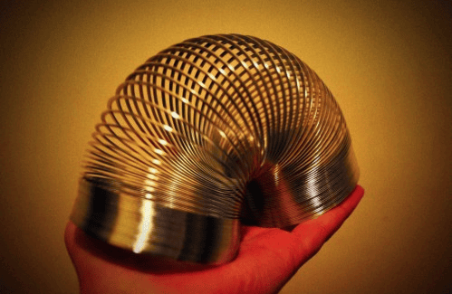
[Image above] Classic Slinky toy. Credit: Louise McLaren; Flickr CC BY 2.0
I can’t help but feel nostalgic when I see retro childhood toys—like the Slinky. I mean… it can “walk” itself down a flight of stairs! I know kids today have resigned toys like this to relic status, but I’ll always have an appreciation for the Slinky’s fun simplicity. Maybe I’m just easy to please.
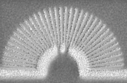
Sometimes a simple design concept can surface in the most surprising and complex places—like this metamaterial hyperlens developed by electrical engineers at the University at Buffalo in New York. The lens, according to a recent university news release, totally resembles the side view of a Slinky suspended in motion.
But these engineers aren’t playing around. Natalia Litchinitser, professor of electrical engineering at the University at Buffalo, co-authored a paper that describes how she and her colleagues are zeroing in on a solution to overcome the diffraction limit so scientists can see even the tiniest things at a resolution sharper than ever before.
Today’s high-res optical systems can resolve objects to about 10,000 nanometers, because diffraction imposes limitations on the sharpness of the magnified image. Scientists really can’t detect the smallest of the small when examining things at a molecular level. Litchinitser and her colleagues posit that this radial-based hyperlens could improve resolution to 250 nanometers or better.
The hyperlens, made from alternating slivers of gold and PMMA (a transparent thermoplastic), is able to overcome the diffraction limit by allowing decaying evanescent waves, which would typically not be captured into propagating waves, to be collected and transmitted using standard microscopes and endoscopes to display a clearer image.

Image shows the radial-based metamaterial hyper lens; the lighter slivers are made of gold and the darker ones are PMMA (a type of transparent thermoplastic). This lens improves resolution of very tiny objects by transforming decaying evanescent waves that would typically not be able to be captured into propagating waves that can be collected and then transmitted, overcoming the diffraction limit. Credit: University at Buffalo
It’s a big deal, because technology like this could, for example, give physicians the ability to detect otherwise difficult-to-find diseases in the earliest stages—which means better odds of treating things like lethal forms of hard-to-see cancers.
And the possibilities reach beyond healthcare. It could lead to advancements in nanoelectronic manufacturing, too, enabling scientists to better study single molecules, which could progress development in fields like physics, chemistry, and materials science.
The paper, published in Nature Communications, is “Experimental demonstration of a non-resonant hyperlens in the visible spectral range” (DOI: 10.1038/ncomms8201).
Mother Nature has many tricks and templates to share about how scientists in biomimetics and materials science can create structures that are stronger and more sophisticated. (Check out this CTT story: Strong, tough, and uncrushable—How Mother Nature designs structural biological materials.) And while programs like the U.S. government’s Materials Genome Initiative strive to speed up the time-to-market for new classes of materials through funding, we’re still not moving fast enough to keep up with the pace of modern technology.
What challenges are you facing in the materials science industry when it comes to engineering materials by design? Share your experiences with us in the comments.
Author
Stephanie Liverani
CTT Categories
- Material Innovations
- Nanomaterials
- Optics


