Last month I shared a story on the work Ohio State University researchers’ development of a computer-controlled “blowtorch” to simulate the high-temperature environment in gas turbine engines (to provide rapid thermal cycling of coatings to predict lifetimes as well as understand the effects of impurities ingested in the engines).
There is more work going on at OSU in the development of materials that can withstand the high temperatures of turbine engines. Referred to as double perovskites, these structures of ceramic oxide crystals may be able to withstand extreme temperatures of up to 1,000ºC without burning because, according to OSU researchers, they’re already oxidized and can retain their properties.
In an article written in OSU’s News in Engineering, the university’s College of Engineering publication, Joan Slattery Wall describes the double-perovskite structure:
The structure of perovskites consists of eight-sided building blocks, or octahedra — atoms that form four-sided pyramids arranged bottom to bottom. Four of these blocks group together like a cube with a different atom nestled in the center. The cubes stack together to form the perovskite crystal. In the double perovskite crystal, the center atom alternates between two different atoms, for example, iron and molybdenum in Sr2FeMoO6, to manipulate the magnetic qualities.
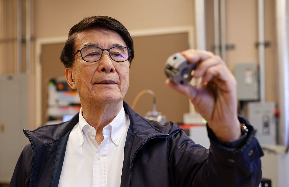
The team is led by Leonard Brillson, a professor in electrical and computer engineering in the school’s Center for Emergent Materials. He explains that the atomic latticework of double perovskites give the structure electromagnetic properties that can sense temperature, pressure, magnetic field and voltage.
“A perovskite is a building block that has special properties and properties you can design just by choosing the right atom to put in it and these can make sensors and computing elements,” Brillson says in the article.
Potential applications for double perovskites include aircraft turbine sensors, computer circuits as well as phased array antennas. The layered structure prevents loss of electrical signal, since that typically occurs between stacked layers. The article states:
“Using oxide molecular beam epitaxy, or MBE, a technique to grow crystals on a substrate, Brillson can ‘spray paint’ atomic layers one at a time as a thin film on a wafer, carefully forming the perovskite crystals to minimize imperfections and allow electrons to pass through the layers with a particular spin. Spin is a property of electrons that a magnetic field can sense and that doubles the amount of information carried through an electrical circuit.”
As a sidenote, Brillson presented a tutorial at ACerS’ 2010 Materials Challenges in Alternative & Renewable Energy. His presentation (coauthored by Sandra DeVincent Wolf and Duane B. Dimos), “Advanced Materials for Our Energy Future,” can be downloaded in PowerPoint format here.
CTT Categories
- Electronics
- Material Innovations
- Nanomaterials


