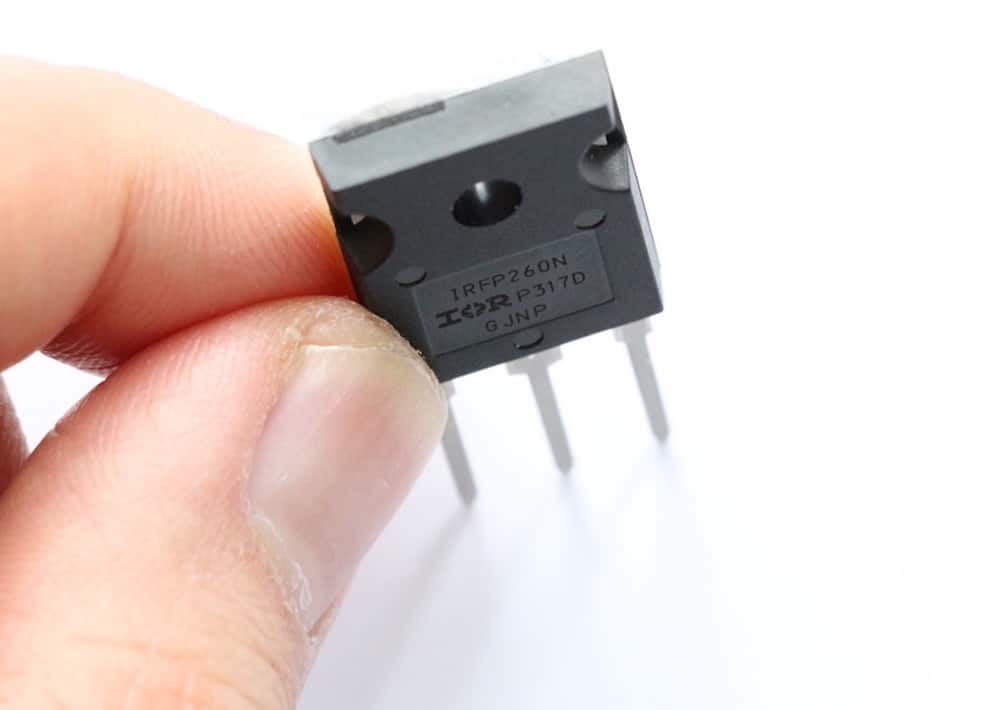
[Image above] Example of a power MOSFET, a specific type of metal–oxide–semiconductor field-effect transistor designed to handle significant power levels. Researchers are working to outfit future MOSFETs with ferroelectric gates to improve their energy efficiency. Credit: Amirhossein Ashrafzadeh, Wikimedia (CC BY-SA 4.0)
When I hear my friends talk about their latest computers or video game consoles, they can ramble off specs for the memory, processor, and graphics card with ease. But ask them what parts inside the device make this performance possible, and few would be able to answer.
Metal–oxide–semiconductor field-effect transistors (MOSFETs) are one component that is integral to modern electronics. Transistors are semiconductor devices used for switching and amplifying electrical signals in electronics. MOSFETs are by far the most widely used transistor in both digital and analog circuits today.
In MOSFETs, electrical current flows between two terminals called the source and drain through either an n-type or p-type channel. Between these two terminals is the gate, an electrode that controls the width of the channel through its voltage.
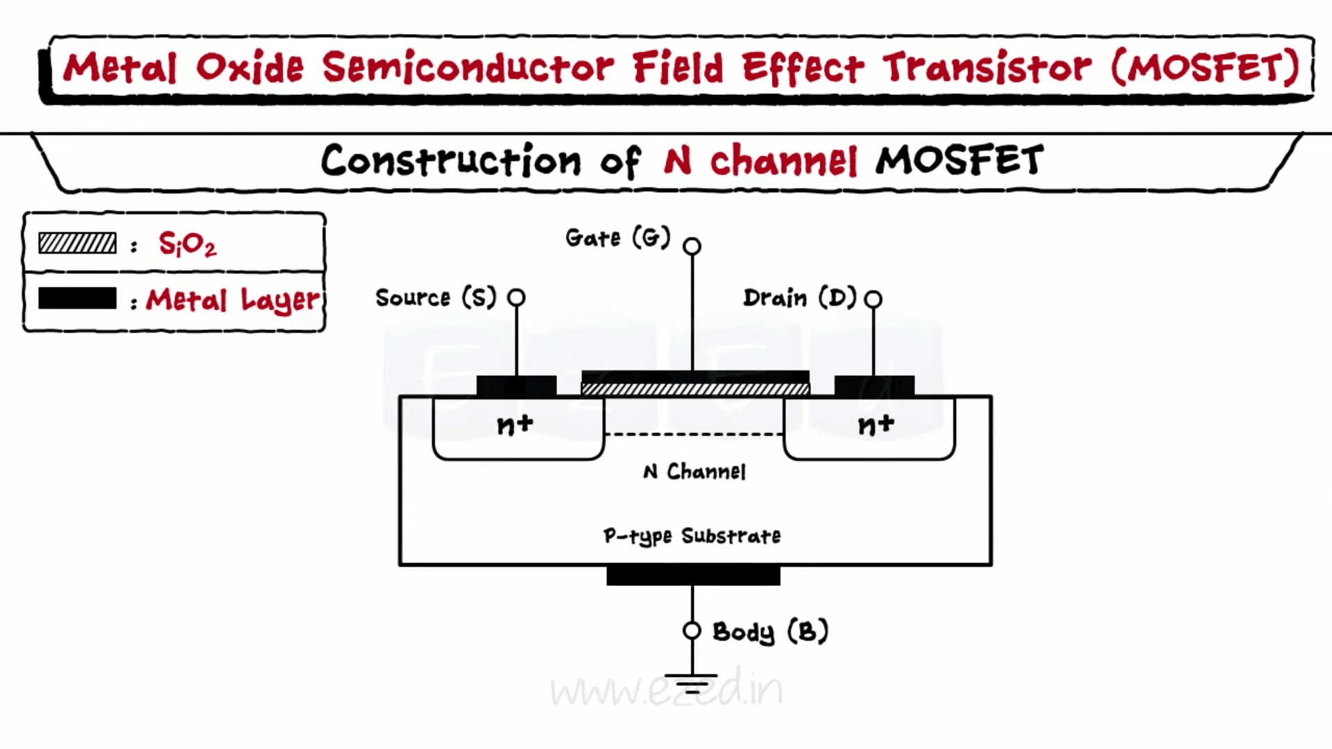
Example of an n-channel MOSFET. Credit: EzEd Channel, YouTube
MOSFETs are considered superior to other types of transistors because of their gate configuration. The gate consists of a metal layer separated from the channel by a thin oxide layer. This insulating oxide layer allows the gate to have very high input impedance, meaning the device draws less current and has lower power dissipation—and thus performs its task of switching and amplifying electrical signals more efficiently.
(Traditionally, the oxide layer consisted solely of silicon dioxide. Now, it is more commonly a multilayer stack consisting of a high-k metal oxide, such as hafnium dioxide, on top of silicon dioxide.)
Since the 1960s, researchers have relied heavily on miniaturization to further improve the efficiency of MOSFETs. However, miniaturization is reaching its limits, particularly regarding the gate oxide thickness and the required voltage for operation.
The thickness of the gate oxide layer and the amount of voltage needed to operate the MOSFET are directly related—reduced thickness allows for reduced voltage, which improves the energy efficiency.
However, below a certain thickness, quantum-mechanical tunneling of electrons through the gate oxide begins to occur, significantly contributing to overall power dissipation. In addition, there is a fundamental lower limit for how much gate voltage is needed to initiate current flow, thus setting a limit on the minimum voltage needed for operation.
Because of these limits to miniaturization, researchers are turning to other techniques, such as materials innovations (e.g., strain engineering) and new device concepts (e.g., fin field-effect transistors), to improve efficiency instead.
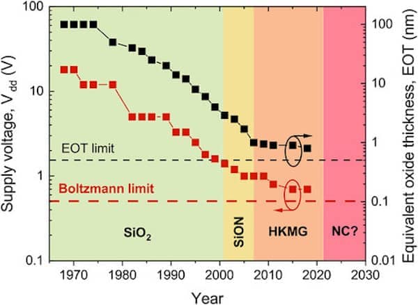
Historic trend of supply voltage and equivalent oxide thickness (EOT) scaling in commercial MOSFET technologies. The black dashed line indicates the EOT limit given by the necessary SiO2 interface between the silicon channel and the high-k material, and the red dashed lines indicates the minimum supply voltage due to the Boltzmann limit. HKMG: high-k metal gate. NC: negative capacitance. Credit: Hoffmann et al., APL Materials (CC BY 4.0)
The potential of negative capacitance transistors
Negative capacitance is one concept that is receiving much attention lately. Capacitance is the ability of a system to store an electric charge. It is determined by how much the system’s charge changes when it is connected to a voltage source.
Due to their structure, MOSFETs have what is known as parasitic or stray capacitances, or areas where capacitance unavoidably occurs due to the proximity of the source, gate, and drain to each other.
Normally, these capacitances are all positive quantities, meaning that changes in the electric flux and the applied electric field occur in the same direction. In other words, when electric flux is reduced, the applied electric field is reduced as well. In practice, this property means that when part of the gate voltage drops across the gate oxide, it reduces the voltage that is “seen” by the channel.
In recent years, researchers have discovered that replacing the high-k metal oxide that rests on top of the thin silicon dioxide layer in the gate with a ferroelectric material may change this behavior.
Ferroelectricity is the property of certain materials to have spontaneous electric polarization that is reversible through application of external electric fields. Ferroelectric materials are a subset of piezoelectric materials, which generate an electric charge in response to an applied mechanical stress.
This property of ferroelectric materials—spontaneous electric polarization—allows them to exhibit negative capacitance behavior, meaning that changes in the electric flux and the applied electric field are opposite each other. In other words, when electric flux is reduced, the applied electric field increases. In practice, this property allows the ferroelectric to serve as a voltage amplifier, so that the voltage “seen” by the channel is larger than the applied gate voltage.
This behavior means less voltage is needed to produce more current—and thus provides a way to surpass the limits set by a traditional oxide layer.
The negative capacitance behavior in ferroelectric materials is thermodynamically unstable, however. So, the big question for researchers right now is how to stabilize this behavior so it can be commercialized.
Michael Hoffmann is studying this question. Hoffmann is a postdoctoral scholar at the University of California, Berkeley. He has studied the idea of negative capacitance electronics since his graduate research at Dresden University of Technology in Germany.
Early last year, Hoffmann and colleagues at TU Dresden published an open-access paper providing a broad look at the field of negative capacitance electronics from a ferroelectric materials perspective.
After that publication, Hoffmann moved to UC Berkeley. In November 2021, he and his advisor, TSMC Distinguished professor of electrical engineering and computer sciences Sayeef Salahuddin, published a new paper that provides a closer look at the recent discoveries of ferroelectricity and negative capacitance in hafnium dioxide (HfO2) and zirconium dioxide (ZrO2)-based thin films with fluorite structure.
As mentioned above, hafnium dioxide is already commonly used in electronic devices (and zirconium dioxide as well). However, only recently have researchers observed ferroelectricity in thin films of these materials with fluorite structures.
Considering contemporary electronics manufacturing is already compatible with hafnium dioxide and zirconium dioxide—in addition to the materials’ relatively large electronic bandgap—ferroelectrics based on thins films of these fluorite-structured materials are especially promising for negative capacitance MOSFETs.
“Due to the early state of this research field, there is still a lot of room for improvement, which will require a focused effort by scientists and engineers at the boundary of materials science, solid-state physics, and device engineering,” Hoffmann and Salahuddin write. “Especially, a better understanding of the microscopic origin of ferroelectricity and negative capacitance in ultrathin fluorite-structure ferroelectrics will be crucial in realizing optimized NC devices.”
Learn more about recent research on ferroelectric materials for negative capacitance electronics in the upcoming April issue of the ACerS Bulletin, which publishes in mid-March.
The first open-access paper, published in APL Materials, is “Progress and future prospects of negative capacitance electronics: A materials perspective” (DOI: 10.1063/5.0032954).
The second paper, published in MRS Bulletin, is “Ferroelectric gate oxides for negative capacitance transistors” (DOI: 10.1557/s43577-021-00208-y).