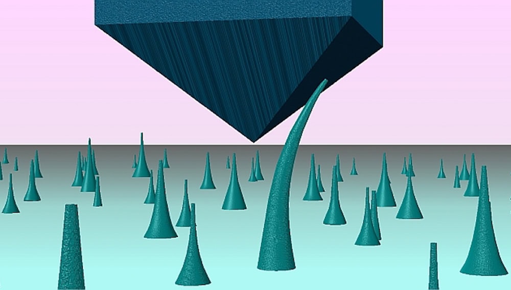
[Image above] A schematic diagram showing the “push to bend” nanomechanical test on a diamond nanoneedle. After an international team of researchers demonstrated this property in 2018, they continued studying the phenomenon and published a follow-up paper this month. Credit: City University of Hong Kong
When developing materials for use in electronic devices, there are a few key qualities that researchers look for. These qualities include
- High thermal conductivity, to allow for efficient extraction of waste heat from the electronic device;
- Good electric charge carrier mobility, to allow for faster device speeds;
- High dielectric breakdown strength, to allow for device operation at higher maximum voltage; and
- Ultrawide bandgap, to allow for device operation at higher frequencies.
Diamond, perhaps surprisingly, fulfills all of these requirements.
“Experimental studies have demonstrated charge-carrier mobilities of >3000 cm2V−1s−1 and thermal conductivities >2000 Wm−1K−1. The material has been predicted to have a breakdown field strength in excess of 10 MVcm−1,” an open-access article from 2008 explains.
Despite these desirable characteristics, researchers struggle to use diamonds in electronic devices because modulating the material’s electronic properties to desired specification is extremely difficult.
Doping is a common way that researchers will modify a material’s electronic properties. However, limitations exist to doping wide bandgap semiconductors, a problem that is exacerbated by diamond’s rigid crystalline structure, which resists conventional doping methods.
Another way to change a material’s electronic properties is through strain engineering, or by deforming a material’s lattice structure. Unfortunately, diamond’s rigid crystalline structure makes this method impractical as well—diamond fractures instead of deforms when subjected to relatively small amount of strain.
How, then, can researchers tailor a diamond’s electronic properties and pave the way for diamond’s use in electronic and optoelectronic devices? An answer lies in one phenomenon we’ve emphasized countless times on CTT—a material may exhibit quite different properties in nanoscale quantities than in bulk form.
Bending on the nanoscale: Microfabricated diamonds for next-generation electronics
In 2018, an international team of researchers led by associate professor Yang Lu at the City University of Hong Kong made headlines when they demonstrated that diamond nanoneedles could undergo fully reversible elastic deformation.
They accomplished this feat by using a nanoindenter diamond tip to bend the diamond nanoneedles, which they observed with a scanning electron microscope. They then combined the real-time bending experiment videos with finite element method analysis to determine that single-crystalline nanodiamonds can achieve maximum local tensile strains up to 9%, which is well above the 0.1%–0.35% strain recorded for bulk diamonds in the past.
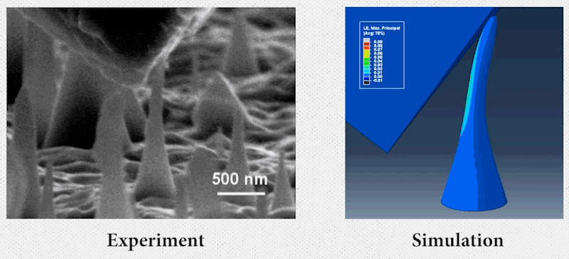
Bending experiment video (left) and simulation (right) of the diamond nanoneedle. Credit: City University of Hong Kong
In the press release, Lu described the team’s feelings as “extremely exciting,” but he noted that this study was only the beginning of the research that could take place. In the almost three years since then, Lu and his colleagues investigated the phenomenon further, and this month they published a follow-up study that more fully explores the possibility of using single-crystalline diamonds in functional electronic devices.
They microfabricated bridge-shaped single-crystalline diamond samples and then uniaxially stretched them in a well-controlled manner. As in the 2018 paper, they combined real-time videos with density functional theory calculations to determine the tensile strain performance.
They determined that the diamond bridges demonstrate a highly uniform, large elastic deformation of about 7.5% strain across the whole gauge section of the specimen, rather than deforming in a localized area. After optimizing the sample geometry and microfabrication process, they increased the maximum uniform tensile strain up to 9.7%, a value that surpassed the maximum local value in the 2018 study.
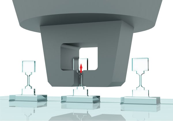
Illustration of the microfabricated diamond bridge samples undergoing tensile strain testing. Credit: Dang Chaoqun, City University of Hong Kong
Of course, the goal of deforming the diamond is to change its electrical properties. So the researchers followed up the tensile strain experiments by investigating how the elastic straining affected the diamond’s bandgap.
Using both calculations and experiments, they concluded that the bandgap generally decreases as the tensile strain increases, with the largest bandgap reduction being a drop from about 5 eV to 3 eV at around 9% strain along a specific crystalline orientation [101].
In addition, their calculations suggest with tensile strains larger than 9% along a specific crystalline orientation [111], the bandgap could transition from being indirect to direct, meaning it would serve more efficiently in optoelectronic applications.
“I believe a new era for diamond is ahead of us,” Lu says in the press release.
The 2018 paper, published in Science, is “Ultralarge elastic deformation of nanoscale diamond” (DOI: 10.1126/science.aar4165).
The 2021 paper, published in Science, is “Achieving large uniform tensile elasticity in microfabricated diamond” (DOI: 10.1126/science.abc4174).