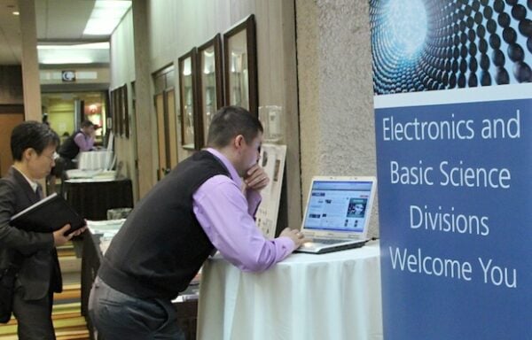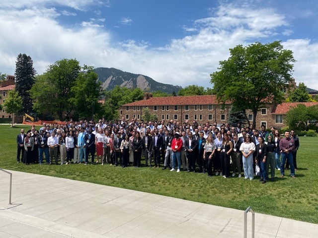
Student presentations of their research in basic science and electronic ceramics are always one of the highlights of EMA. Photo from 2013 meeting. Both photos credit: ACerS.
ACerS has a busy 2014 meetings schedule, kicking off Jan 22–24 with Electronic Materials and Applications 2014 in Orlando, Fla. Attendance for the event grew significantly in 2013, and nearly 300 scientists and engineers are expected to attend this year’s edition.
Jointly organized by the Society’s Electronics and Basic Science divisions, the upcoming conference features new programming covering commercialization of electroceramics and computational design of electronic materials. Also new is a tutorial recognizing the importance of interfaces in electroceramic materials.
A session entitled “Functional and Multifunctional Electroceramics for Commercialization” recognizes that moving an innovation from invention to commercialization can be a challenge. This symposium not only covers advances in functional and multifunctional electroceramics but also their potential commercial opportunities in energy storage, conversion, and harvesting; detectors and sensors; electronics packaging and interconnect applications; and more.
The session entitled “Computational Design of Electronic Materials” recognizes the importance of reducing the cost, risks, and time needed for materials discovery. Computational techniques can do all that, and form the core of the US Materials Genome Initiative. Scientists and engineers from academia, industry, and national laboratories will discuss the current state of and future outlook for computational modeling and informatics for electronic materials, including
- Emerging strategies for discovering and designing new electronic materials;
- High-throughput data generation and screening via first principles;
- Data mining, knowledge discovery, and informatics;
- Statistical methods and machine learning for accelerating materials property predictions;
- Modeling at different (and across) scales.
Also new is a tutorial on interfaces. Instructors Dominique Chastain and Wayne D. Kaplan will provide an introduction to many of the topics to be discussed in more detail during EMA’s “Structure and Properties of Interfaces in Electronic Materials” conference session.
As always, EMA 2014 will include plenary sessions, poster sessions, highlights of student research in basic science and electronic ceramics, and plenty of networking opportunities. For more information, including the full technical program, visit the EMA 2014 website.
Author
Jim Destfani
Spotlight Categories
- Meeting Highlights
Divisions
- Basic Science
- Electronics


