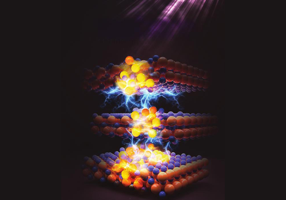
[Image above] Artist’s impression of electrically driven solid-state amorphization in ferroelectric β″-phase indium selenide. The lightning bolts indicate electrical spikes from piezoelectricity-induced mechanical shocks, which transition the material to a glassy phase. Credit: Aakanksha Jain; Indian Institute of Science, Bengaluru
With energy demands surging in the computing sector due to the expansion of data centers and artificial intelligence models, new materials with better thermal and electrical properties are needed to improve the efficiency and reduce the power consumption of electronic systems.
Earlier this month, we talked about the potential of some oxide semiconductor materials to reduce the power consumption of high-performance computing systems. Today, we will talk about the potential of a newer semiconductor material—indium selenide—to reduce the power consumption of traditional optical storage media.
Indium selenide is sometimes called the “golden” semiconductor due to its combination of graphene-like (extreme thinness) and silicon-like (high electron mobility) properties. In contrast to these other materials, however, indium selenide exhibits a remarkably tunable bandgap, due in part to its multiple stable crystalline phases.
Large-scale production of 2D indium selenide for wafer-scale integration has remained elusive due to difficulties maintaining an ideal atomic ratio between indium and selenium during synthesis. While some groups work on overcoming this hurdle, others continue to investigate the full extent of indium selenide’s unique properties and capabilities.
In November 2024, researchers from the University of Pennsylvania, along with colleagues from Massachusetts Institute of Technology and Indian Institute of Science, Bengaluru, published a paper describing a novel capability of ferroelectric β″-phase indium selenide—the ability to undergo solid-state amorphization through direct-current stimulation.
Traditional optical storage media devices such as CDs, DVDs, and Blu-ray discs store and erase data by switching a material, typically germanium antimony telluride, between its crystalline and glassy phases. This switch is triggered using laser pulses to rapidly heat and quench the phase-change material, during which time it passes through an intermediate liquid phase.
The rapid heating and cooling of phase-change materials often requires temperatures exceeding 500°C, which unsurprisingly is energy intensive. If the phase-change material could achieve a solid-state transition between the crystalline and glassy phases—no melting required—the amount of power needed for memory storage could be greatly reduced.
There are several examples of researchers using mechanical methods to achieve solid-state amorphization, such as here and here. But if researchers could use electricity to induce this transition instead, adapting the process for use in optical storage media would be easier and open the possibility for low-power device applications.
Electrically driven solid-state amorphization has been reported in single-crystalline nanowires of germanium telluride, such as here and here. However, the material can exhibit metallic conductivity upon transitioning, which complicates the use of this method and requires electricity to be delivered in pulses.
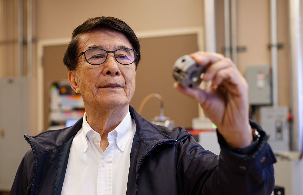
When Gaurav Modi, former Ph.D. student at the University of Pennsylvania and first author of the recent paper, first attempted electrical stimulation of indium selenide nanowires, he was shocked to observe that the solid-state transition could be induced through continuous, rather than pulsed, current.
“I actually thought that I might have damaged the material,” he says in a press release. “Normally, you would need electrical pulses to induce any kind of amorphization, and here, a continuous current had disrupted the crystalline structure, which shouldn’t have happened.”
Modi and his coauthors then used a suite of in-situ microscopy tools to uncover the mechanism enabling this transition.
They discovered that when a continuous current is passed parallel to the 2D indium selenide’s layers, the layers slide against each other in different directions. This sliding causes the formation of many domains bound by defective regions, and when multiple defects intersect in a small nanoscopic region, the structural integrity of the crystal collapses to form glass locally.
The collapse of these local regions triggers an avalanche effect, whereby more domain boundaries are created and then collapse. The avalanche stops when the entire material turns into glass.
“It’s just goosebumps stuff to see all of these factors come to life and play together, at different length scales in an electron microscope,” says second author Shubham Parate, Ph.D. student at Indian Institute of Science, Bengaluru, in the press release.
According to the press release, the authors now plan to investigate integrating ferroelectric β″-phase indium selenide on electronic chips.
The paper, published in Nature, is “Electrically driven long-range solid-state amorphization in ferroic In2Se3” (DOI: 10.1038/s41586-024-08156-8).