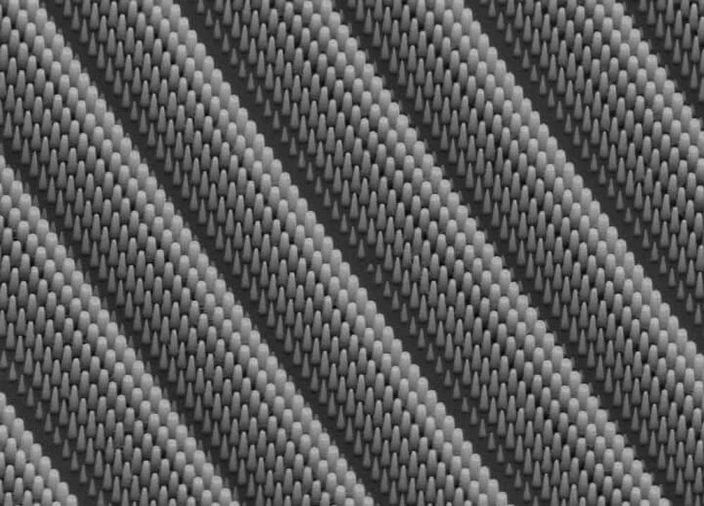
[Image above] Scanning electron microscopy image of an “imperfect” silica metasurface fabricated at Harvard University, in which the final nanopillar shapes are not the desired cylindrical geometry. Credit: John A. Paulson School of Engineering and Applied Sciences
Though nanomaterials have unwittingly played a role in materials advancements for centuries, it is only within the past 50 years that we gained the techniques and technologies to engineer materials purposefully on this scale. Nanoscience now plays a critical role in numerous industries, as demonstrated at this year’s Golden Jubilee Celebration of the International Conference and Expo on Advanced Ceramics and Composites.
Yet even as we celebrate the achievements in engineered ceramic and glass components made in the last few decades, scientists continue to push the envelope on what is possible thanks to micro- and nanoscale engineering. The January/February 2026 issue of the ACerS Bulletin provided a deep dive into some of these innovation areas, and today’s CTT explores another area ripe for development: photonic lenses.
Photonic lenses are advanced optical components for light manipulation. They consist of repeating structures that enable, inhibit, or direct light flow, similar to how semiconductors control electron behavior.
Traditionally, materials with a high refractive index are preferred for photonic lenses because they can bend light more effectively, enabling the creation of thinner, lighter, and more compact optical components. Gallium arsenide, silicon nitride, and titanium dioxide are all examples of high-refractive-index materials.
Silica glass, on the other hand, has a low refractive index. So, even though glass is the ideal choice for many optical applications, usually it is not preferred for manipulating light on the micro- or nanoscale. It offers other advantages, though, such as robustness under high-power laser illumination and compatibility with traditional integrated circuit manufacturing processes. It can thus be a good choice for some photonic lenses depending on the intended optical functionality.
In May 2025, a team of researchers from China, Denmark, and Singapore made a significant discovery: despite its low refractive index, silica glass can sometimes rival high-refractive-index materials in reflectance if fabricated with enough repeating units and structural uniformity. This discovery suggests that the design of silica glass, rather than its inherently low refractive index, may be the deciding factor when choosing materials for photonic lenses.
The follow-up question is then: What amount of structural uniformity is required to achieve this performance? Perhaps surprisingly, silica glass can accommodate a fair number of imperfections and still perform “remarkably well,” according to researchers in Harvard University’s John A. Paulson School of Engineering and Applied Sciences (SEAS).
The researchers are led by Federico Capasso, the Robert L. Wallace Professor of Applied Physics and Vinton Hayes Senior Research Fellow in Electrical Engineering at Harvard SEAS. His group has investigated the fabrication and application of glass metalenses for years. (Metalenses are a type of flat photonic lens constructed of nanoscale arrays of columns or fin-like structures.)
In an open-access paper published in December 2025, the Harvard SEAS researchers identified and experimentally verified regimes where silica glass surpasses titanium dioxide, a high-refractive-index material. They determined that unlike high-refractive-index materials, each etched nanopillar of silica supports only a single, clean path of light. This “single-mode” regime does not suffer from interference between multiple paths of light, so the desired phase profile and transmission of light can be achieved.
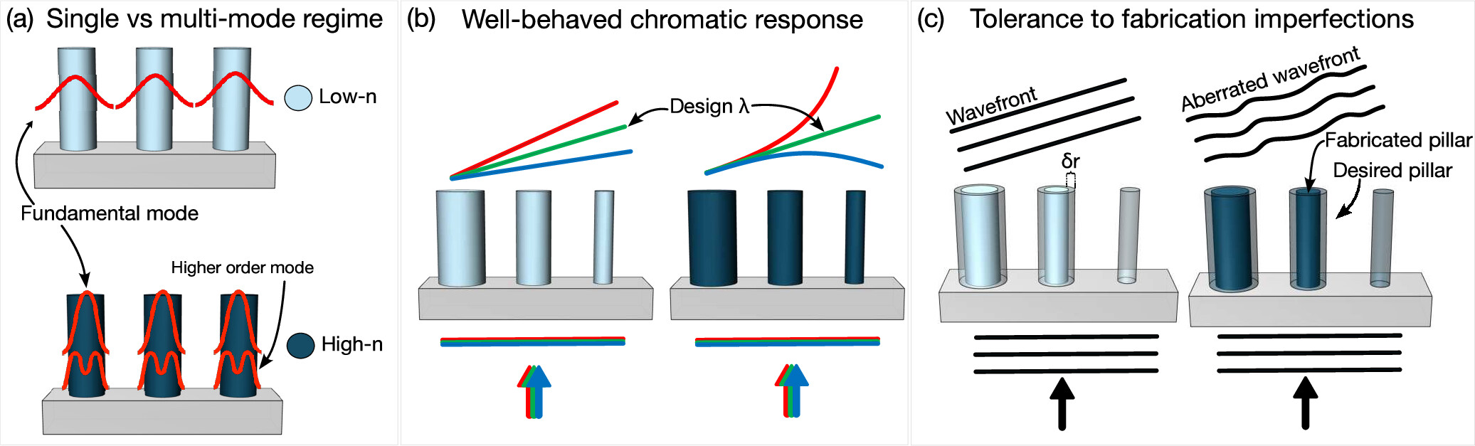
Illustration showing the key advantages of low-refractive-index glass metasurfaces. a) Single-mode and multimode Bloch representation in materials with low (glass) and high (titanium dioxide) refractive indices. b) Broadband behavior of glass and titanium dioxide metasurfaces. c) Robustness of optical functionality to fabrication error δr in glass versus titanium dioxide. Credit: Sacchi et al., Nano Letters (CC BY-NC-ND 4.0)
The researchers created several types of metasurfaces out of silica and titanium dioxide, including metagratings, metalenses, and vortex phase plates. In each case, the lack of multimode light propagation among the silica nanopillars meant the desired optical performance could be achieved even with a significantly higher number of fabrication errors, in contrast to the titanium dioxide-based metasurfaces.
Specifically, “the silica gratings and lenses exhibited nearly constant efficiency under ±50 nm of lithographic deviation (including sidewall tapering), a level of error that would severely degrade titanium dioxide devices,” the researchers write.
In a Harvard SEAS press release, author Marco Piccardo, former Capasso group member and now faculty member at the University of Lisbon, explains that the advantages of silica photonic lenses were partly overlooked until now because of major obstacles in nanofabrication.
“As we are able now to etch very tall nanopillars with vertical sidewalls, we can make full use of this low-index platform, with all its benefits for exciting applications,” Piccardo says.
The open-access paper, published in Nano Letters, is “Silica meta-optics: When high performance does not need a high index” (DOI: 10.1021/acs.nanolett.5c04960).