[Image above] If ammonium ions are not properly removed from semiconductor wastewater before it is discharged, these ions can accelerate eutrophication of aquatic environments, or the excessive growth of algal and plant matter caused by an overabundance of minerals and nutrients. Credit: eutrophication&hypoxia, Flickr (CC BY 2.0)
Everyone is talking about the semiconductor manufacturing mega-site that Intel is planning to build on the outskirts of Columbus, Ohio. While much of this conversation is focused on the economic impacts it will have on the area, I’ve seen questions raised about the possible environmental impacts as well.
Semiconductor chip processing and manufacturing is a very water- and energy-intensive process. Look no further than Intel’s existing 700-acre campus in Ocotillo, Arizona, as an example—in the first three months of 2021, this single fabrication plant consumed 927 million gallons of fresh water, enough to fill about 1,400 Olympic swimming pools, and used 561 million kilowatt-hours of energy.
The semiconductor industry is working to address these heavy requirements and lessen its environmental impact. For example, in 2020, Taiwan Semiconductor Manufacturing Company became the world’s first semiconductor company to join RE100, a global initiative to move away from widespread reliance on fossil fuels and toward 100% renewable electricity to power operations. In addition, numerous semiconductor companies are improving their water recycling and reuse capabilities to reduce their total freshwater consumption.
Filtering of semiconductor wastewater is a key part of the water recycling and reuse process. Semiconductor wastewater contains a wide range of organic and inorganic impurities removed during the manufacturing process, such as hydrofluoric acid, phosphoric acid, ammonium hydroxide, photoresists, and strippers.
Removal of ammonium ions from the wastewater is a particular concern for chip manufacturers. If ammonium ions are not properly removed before the wastewater is discharged, these ions can accelerate eutrophication of aquatic environments, which is when bodies of water experience excessive plant and algal growth due to an overadundance of minerals and nutrients, leading to oxygen depletion and so-called “dead zones.”
Biological treatment using nitrification and denitrification is the most prevalent method for ammonium removal from semiconductor wastewater. “However, the biological transformation of ammonium is limited by its high toxicity and low biodegradability in semiconductor wastewaters. … Given the complexity and toxicity of semiconductor wastewater, membrane-based separation can be an attractive option for ammonium removal,” researchers write in a recent paper.
The researchers come from Ewha Womans University, the Korea Institute of Science and Technology, and the Korea Institute of Materials Science in South Korea. In their paper, they look at the potential of graphene oxide-based nanofiltration membranes to remove ammonium from semiconductor wastewater.
They explain that ceramic membranes have received a lot of attention lately for treating different types of wastewaters due to their high chemical, thermal, and structural stability and their antifouling nature compared to conventional polymeric membranes. However, ceramic membranes have not been widely investigated for semiconductor wastewater treatment specifically.
The researchers chose to focus on graphene oxide-based nanofiltration membranes for several reasons. One, to effectively remove ammonium ions, a very small pore size is needed. Thus, nanofiltration membranes need to be used, in contrast to larger micro- or ultrafiltration membranes.
Currently, development of ceramic nanofiltration membranes that enable effective retention of ionic compounds and high water permeability is limited. Fortunately, studies on graphene oxide have shown it holds great potential as a material for ceramic nanofiltration membranes, so the researchers chose graphene oxide for their study.
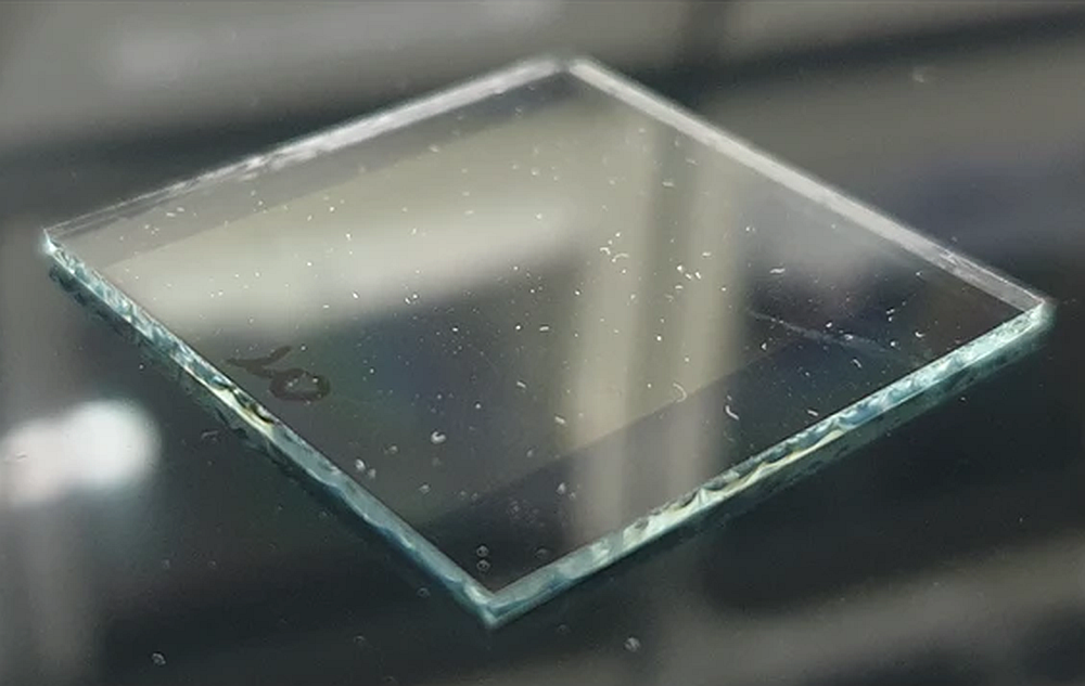
The researchers developed a graphene oxide-based nanofiltration membrane using a cyclical layer-by-layer assembly process to deposit graphene oxide–polyethyleneimine bilayers on top of a ceramic ultrafiltration membrane. They chose this approach based on previous studies showing it can improve stability of the graphene oxide layer.
The researchers fabricated several nanofiltration membranes featuring differing numbers of graphene oxide–polyethyleneimine bilayers. Then, they analyzed the ammonium rejection rates and fouling potential of each membrane using both simulated and real semiconductor wastewater.
Based on the filtration experiments, the researchers concluded that the graphene oxide-based nanofiltration membranes demonstrated significantly improved performance compared to an uncoated ceramic ultrafiltration membrane.
Specifically, graphene oxide-based nanofiltration membranes with three graphene oxide–polyethyleneimine bilayers exhibited 8.4- and 3.2-times higher ammonium removal with simulated and real semiconductor wastewater, respectively, compared to the ceramic ultrafiltration membrane. Plus, flux recovery increased from 39.1% in the ceramic ultrafiltration membrane to 71.0% and 90.8% for the three- and ten-bilayer graphene oxide-based nanofiltration membranes, respectively.
“The low-fouling [graphene oxide-based nanofiltration membranes] developed in this study are effective and promising options for the removal of ammonium ions from semiconductor wastewater,” the researchers conclude.
The paper, published in Chemosphere, is “Investigating the potential of ammonium retention by graphene oxide ceramic nanofiltration membranes for the treatment of semiconductor wastewater” (DOI: 10.1016/j.chemosphere.2021.131745).
Author
Lisa McDonald
CTT Categories
- Environment
- Manufacturing


