 [Image above] Will this little light-bending silicon chip change the future—or at least our smartphones? Credit: Caltech.
When the Apple iPhone 5 was about to be released in late 2012, and speculations about its new features were running amuck, I heard rumors of a holographic display. At the time I thought that was completely ridiculous, and apparently so did tech sites like Geek.com.
Although Geek.com experts scoffed at the idea, new research suggests that you may want to retract that “ridiculous” adjective and insert “feasible” instead.
California Institute of Technology engineers recently reported the ability to bend light with only a silicon chip, an early step toward simple and cost-effective projection capabilities in a variety of applications, including your smartphone. The research was led by electrical engineering professor Ali Hajimiri.
Traditional LCD projectors pass light through pixels to project holographic images and rely on moving parts and lenses to adjust light beams. In contrast, the new Caltech chip uses an integrated optical phased array (OPA) to project the image with a single LED and no mechanical parts.
The scientists took advantage of light coherence, the wave property behind interference. “By changing the relative timing of the waves, you can change the direction of the light beam,” says Hajimiri in a Caltech press release.
The press release continues, “For example, if 10 people kneeling in line by a swimming pool slap the water at the exact same instant, they will make one big wave that travels directly away from them. But if the 10 separate slaps are staggered—each person hitting the water a half a second after the last—there will still be one big, combined wave, but with the wave bending to travel at an angle.”
By taking control of the waves, the researchers made a big splash. They fabricated a silicon chip that can bend and manipulate light waves—and thus change the direction of a light beam—with a series of phase shifters. The electronic data of the image to be projected is first converted into adjustable electrical currents. The intensity of those electrical currents subsequently guides the timing of the light waves hitting the silicon chip. The waves strike the chip’s array elements, which project light beams that combine coherently mid-air to form a projection.
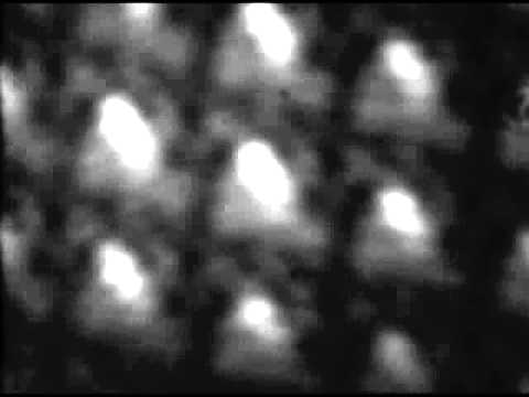
While the chip doesn’t project static light beams in one location, it draws them very quickly and repeatedly so that your eye perceives a single image. Watch the video below to see how little projected triangles look when you slow them down, and then how your eye perceives the fast bursts of light.

Credit: Caltech, Youtube
“The new thing about our work is really that we can do this on a tiny, one-millimeter-square silicon chip, and the fact that we can do it very rapidly—rapidly enough to form images, since we phase-shift electronically in two dimensions,” graduate student Behrooz Abiri says in the press release.
The scientists performed initial tests using infared light on silicon chips, but note that other semiconductors could be used to expand applications into the visible light spectrum. So far the scientists can only project simple shapes or letters, but they are also working on larger chips to raise the complexity and resolution of projections.
Hopefully tiny projectors can eventually be affixed to our personal devices and much more. “I don’t want to limit the device to just a few purposes,” Hajimiri says. “The beauty of this thing is that these chips are small and can be made at a very low cost—and this opens up lots of interesting possibilities.”
The scientists presented their work at Optical Fiber Communication (OFC) conference in San Francisco earlier this month.
Perhaps R2D2’s hologram isn’t so crazy after all…
Author
April Gocha
CTT Categories
- Electronics
- Material Innovations
- Optics


