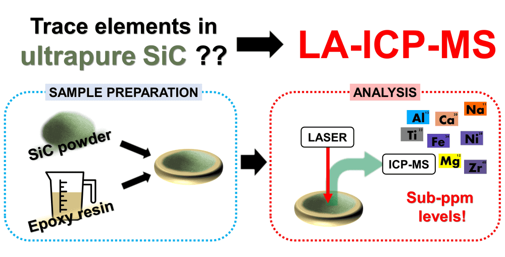
[Image above] Graphical abstract for a new analytical protocol to determine purity of silicon carbide. Credit: Spanu et al., Molecules (CC BY 4.0)
Governments are not the only ones with an eye toward the expansion of domestic semiconductor manufacturing hubs. Materials suppliers are also keeping close tabs on the industry because increased production will increase demand for high-purity materials.
High-purity chemicals and materials are essential in manufacturing microelectronics devices to ensure consistent quality and performance during mass production. Even trace contaminants can adversely affect the efficiency of devices.
Materials suppliers are working to expand their offerings of higher purity materials, such as Almatis GmbH, which reported its progress on generating higher purity alumina in the April 2023 Bulletin.
But as manufacturers push to offer higher purity rates up to more than 99.9%, verifying the purity of the materials becomes an increasingly difficult task.
Take, for example, silicon carbide. Achieving a 99.999% purity means that the sum of all impurities cannot exceed the concentration of 10 mg/kg.
Currently, the most common approach for determining silicon carbide purity involves dissolving the sample and then analyzing it through inductively coupled plasma mass spectrometry or inductively coupled optical emission spectrometry.
There are two drawbacks to this approach:
- Silicon carbide is extremely inert, so dissolving it requires harsh conditions, such as microwave acid digestion or alkaline melting.
- The dissolution of silicon carbide through these methods can lead to high background or blank signals.
Thus, determination of trace elements using wet digestion methods is difficult. The detection limits that are generally reported for this approach are higher than mg/kg levels.
Analytical techniques that work directly on the sample without pretreatment are another option for trace element analysis. For example, glow discharge mass spectrometry (GD-MS) can yield highly sensitive measurements in the order of tens or hundreds of µg/kg. But this technique can be very costly, which inhibits its adoption in industry, an environment that requires high-throughput analysis to be conducted on numerous samples.
Laser ablation paired with inductively coupled plasma mass spectrometry (LA-ICP-MS) has been proposed as a simpler and more affordable direct analytical method. The instrumental cost of LA-ICP-MS is at least four times lower than that of double-focusing GD-MS. Plus, it can provide reliable quantitative information down to mg/kg and sub-mg/kg levels.
To date, few studies have reported on the use of LA-ICP-MS to analyze silicon carbide purity. So, there are numerous questions that must be addressed to realize the potential of this technique, such as identifying universal sample preparation and calibration strategies.
In an open-access paper, researchers in Italy and Norway developed an optimized protocol for using LA-ICP-MS to quantify trace elements in ultrapure silicon carbide.
The first step was preparing the sample for analysis. For good quantitative analysis with laser ablation, a fundamental requirement is that the sample be as compact and planar as possible. This structure allows for the laser beam to hit perpendicularly, an angle which favors a better and more reproducible ablation of the material.
“Therefore, such powdered samples should be pretreated to have a somewhat enhanced degree of compactness,” the researchers write.
They compacted silicon carbide powder using two different strategies:
- The fabrication of binder-free silicon carbide tablets, as proposed by Zhou et al. (2013)
- The embedding of silicon carbide powder in epoxy resin (newly developed strategy).
The first strategy, which involved finely grinding silicon carbide powder in an agate mortar, was not able to obtain a sufficient degree of compactness for LA-ICP-MS analysis. An additional thermal treatment was needed to induce partial sintering of the pressed powders.
Even then, analysis revealed that the process of grinding the silicon carbide in an agate mortar contaminated the sample, “a bulk contamination that cannot be lowered by preventive ablation cleanings,” the researchers write.
This result led them to develop the second strategy mentioned above. In this case, both grains and fine powders of silicon carbide were embedded in epoxy resin. The samples were then cut, polished, and externally cleaned using hydrochloric acid 0.1 M.
Compared to the binder-free tablets, the embedded epoxy samples were highly compact and could be handled without special precautions. Additionally, during optimization of the laser ablation parameters, the researchers immediately observed the total absence of unwanted powder lifting, which ensured much more stable and less noisy signals.
Using GD-MS as a reference technique, the researchers optimized sample preparation and ablation protocols and ultimately achieved highly precise results with LA-ICP-MS for sub-ppm concentrations.
“…the extremely simplified sample work-up of the proposed LA-ICP-MS approach represents a significant advancement with respect to previous literature,” the researchers write.
In the future, they plan to further optimize sample preparation (e.g., through preliminary grinding with a boron carbide mortar) and introduce a multipoint calibration technique, which would allow them to extend the number of elements to be quantified.
The open-access paper, published in Molecules, is “Tackling the challenging determination of trace elements in ultrapure silicon carbide by LA-ICP-MS” (DOI: 10.3390/molecules28062845).