![]()
[Image above] A newly designed adhesive tape tunable via ultraviolet light can transfer 2D materials onto a range of different substrates, including silicon, ceramic, glass, and plastic. Credit: Ago Lab, Kyushu University
When University of Manchester professors Andre Geim and Konstantin Novoselov conducted their Nobel Prize winning experimental confirmation and analysis of graphene in 2004, their method for isolating the graphene was stunningly simple—they removed a single layer of carbon atoms from bulk graphite using regular adhesive tape.
Flash forward to today and graphene production is much more elaborate. Rather than using mechanical methods to separate out graphene flakes, wet chemical exfoliation techniques are the go-to approach for mass production due to providing more control over graphene purity and number of layers.
However, after graphene is synthesized, it must be transferred from the production chamber onto various target substrates for application. And current transfer methods tend to degrade the graphene’s quality.
For example, thin polymer support layers are regularly used to transfer graphene grown through chemical vapor deposition. After transfer, the support layer is removed, usually through dissolution with organic solvents. This process leaves behind residues on the graphene’s surface plus limits the choice of target substrates (i.e., no flexible plastics).
In a new open-access paper, researchers led by Kyushu University went back to the basics and showed that adhesive tape, though not the answer to mass graphene production, may be an ideal solution for mass graphene transfer.
The adhesive tape in this case was not simply off-the-shelf Scotch tape, such as Geim and Novoselov used in their 2004 experiments. Instead, the researchers worked with Japanese company Nitto Denko to develop a tape with an adhesive force tunable through ultraviolet light illumination.
As illustrated in the figure below, the tape is first attached to the as-grown graphene and then illuminated with ultraviolet light. The light hardens the adhesive layer while also greatly weakening the graphene–adhesive interaction, setting the stage for the graphene’s eventual release.
The tape/graphene stack is detached from the original substrate by electrochemical delamination and then washed with deionized water. Next, the stack is gently placed on the new substrate and baked at 90°C. Finally, the tape is slowly peeled off the stack at 80°C, leaving behind monolayer graphene.
Illustration of the new tape-based transfer process for monolayer graphene. In this case, the graphene was grown on a Cu(111) thin film and transferred to a SiO2/Si substrate. Credit: Nakatani et al., Nature Electronics (CC BY 4.0)
Analysis of the graphene via optical microscopy revealed a pristine product without damages or contamination. However, many defects were observed in the areas that missed being illuminated, “demonstrating the efficient control of adhesive force by UV light,” the researchers write.
They used the ultraviolet light-sensitive tape to transfer both small and large amounts of graphene, from millimeter-sized areas up to wafer scales (see video below). They note that once the graphene is attached to the tape, it can be easily cut into different sizes and shapes before the graphene is released.
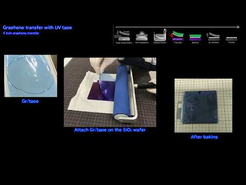
Wafer-scale transfer process of monolayer graphene using adhesive tape tuned by ultraviolet light. Credit: Nakatani et al., Nature Electronics (CC BY 4.0)
The ultraviolet light-sensitive tape transfer method is not only applicable to graphene. The researchers also transferred semiconducting transition metal dichalcogenides and multilayer hexagonal boron nitride using this method, though the adhesive composition needed to be modified to ensure proper attachment and release of different materials.
In a press release, lead author Hiroki Ago, professor in Kyushu University’s Global Innovation Center, says their method “could fundamentally change the style of research and accelerate the commercial development of 2D materials.”
To date, the researchers have successfully transferred graphene wafers up to 10 cm in diameter. They are working to expand the size of the ultraviolet light-sensitive tape to the scale needed for manufacturers.
Plus, they aim to improve stability of the 2D materials on the ultraviolet light-sensitive tapes so the tapes can be distributed to other end users, such as scientists at different institutions, with the materials already attached.
The open-access paper, published in Nature Electronics, is “Ready-to-transfer two-dimensional materials using tunable adhesive force tapes” (DOI: 10.1038/s41928-024-01121-3).