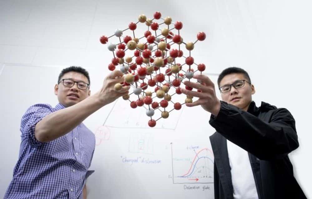
[Image above] University of Toronto professor Yu Zou, left, and Ph.D. candidate Mingqiang Li hold an atomic structure model of a zinc sulfide crystal, which was the ceramic used in their new study on controlling dislocation motion via electric fields. Credit: Adrian So, University of Toronto
There are numerous ways that researchers can unlock versatile and unexpected functional and mechanical properties in ceramics. Engineering dislocations into ceramics is a nascent method that is gaining traction, as detailed in the cover story of the June/July Bulletin.
Dislocations are one-dimensional line defects that are the main carriers of plastic deformation in crystalline solids. Since about 2003, various studies have shown that a wide range of properties can be tuned by engineering dislocations, including electrical properties, thermal properties, and plastic behavior.
Due to the brittleness of most ceramics, engineering dislocations into ceramics without crack formation is a challenge. To date, researchers have engineered dislocations in ceramics mainly through interface design, processing, and mechanical deformation. Among these approaches, mechanical deformation offers the best opportunity for aligning dislocations along specific slip planes.
While some studies have demonstrated that electric fields and light exposure can affect the motion of dislocations in ceramics, the principal driving force of motion in these cases was still mechanical stress. Proof that dislocation motion can be controlled solely by a nonmechanical stimulus remained elusive—until now.
In a new paper published in Nature Materials, an international group of researchers presented real-time observations of dislocation motion in a single-crystalline zinc sulfide that was controlled using only an external electric field.
The researchers come from the University of Toronto and Dalhousie University (Canada), Iowa State University (U.S.), and Peking University (China). In the paper, they explain that recent advances in in-situ transmission electron microscopy (TEM) are what allowed them to observe the motion of dislocations in zinc sulfide.
The researchers used atomic-scale characterization of the dislocation cores and density functional theory calculations of the dislocation glide barriers to explain how the electric field caused the dislocations to move.
They also ruled out the possibility of other effects influencing the dislocation motion by pointing out some key parts in the in-situ TEM footage (see example footage here). Specifically,
- The observation of dislocations moving back and forth eliminates the Joule heating mechanism because “the thermal stress arising from Joule heating is independent of the direction of the applied electric field.”
- The possibility that electron wind force plays a dominant role in the motion was ruled out because “the different types of dislocations move in opposite directions under the same voltage.”
- Though electron beam irradiation is reported to possibly enhance dislocation mobility, in this study, “even when the electron beam is off, we still observe that the positions of the 30° dislocations are changed under an electric field.”
A University of Toronto press release reports that the researchers plan to explore the possibility of using this technique to engineer dislocations in other types of crystals.
The paper, published in Nature Materials, is “Harnessing dislocation motion using an electric field” (DOI: 10.1038/s41563-023-01572-7).