[Image above] Representation of a 2D ferroelectric material. Credit: Suraj Cheema, UC Berkeley
With domestic semiconductor manufacturing becoming a focus for countries around the world, it also sheds light on the fact that a traditional guiding principle for chip manufacturing—Moore’s Law—no longer holds true.
Moore’s Law is a prediction made by Intel cofounder Gordon Moore in 1965. Based on observation, he extrapolated that computing would dramatically increase in power while decreasing in relative cost at an exponential pace. This prediction would be realized through doubling the number of transistors (a semiconductor device used to amplify or switch electrical signals and power) on a microchip roughly every two years.
However, in recent years, miniaturization of transistors is pushing up against fundamental limits.
The most widely used transistor type is the metal–oxide–semiconductor field-effect transistor (MOSFET). In MOSFETs, electrical current flows between two terminals called the source and drain through either an n-type or p-type channel. Between these two terminals is the gate, an electrode that controls the width of the channel through its voltage.
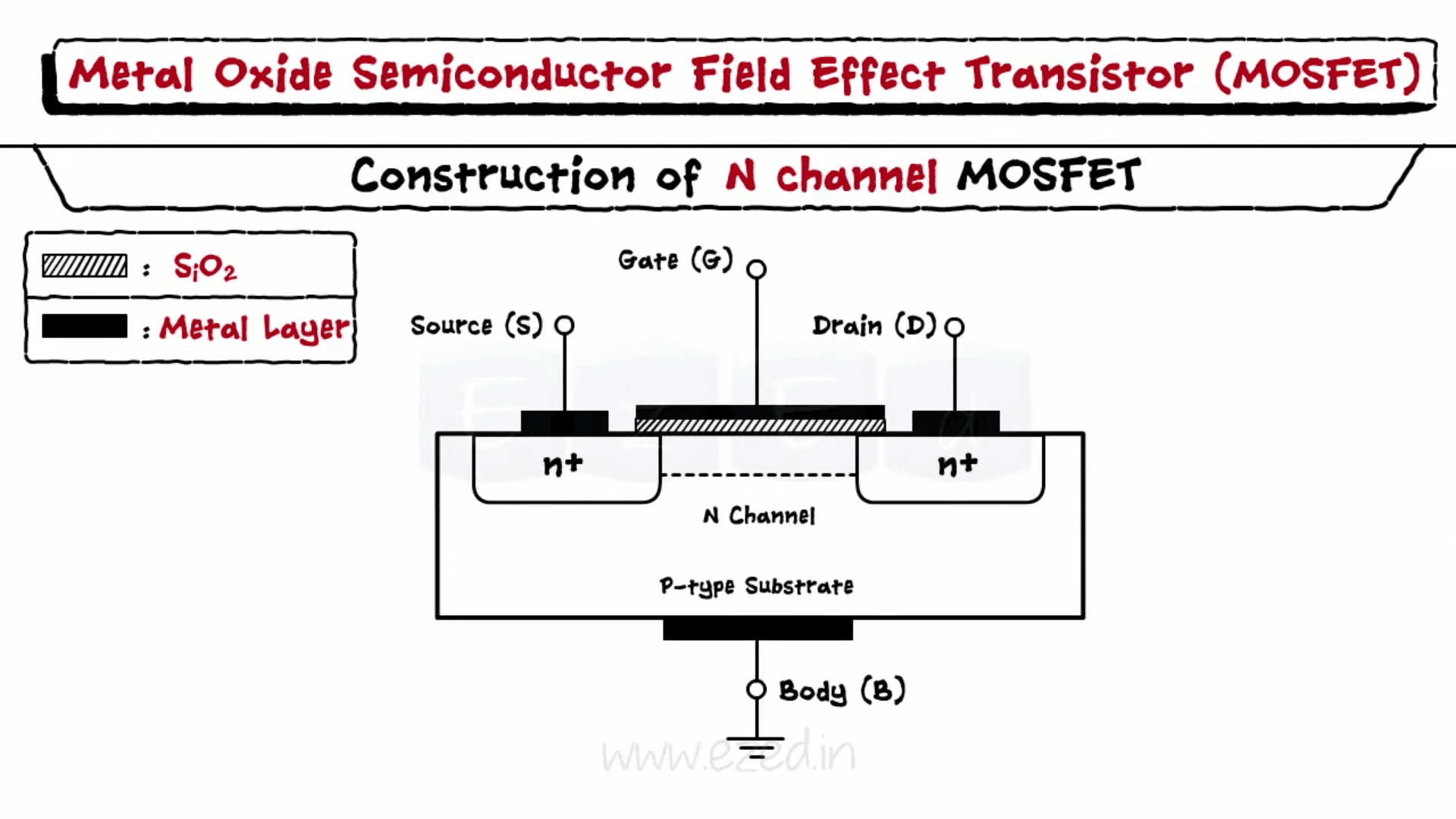
Example of an n-channel MOSFET. Credit: EzEd Channel, YouTube
The gate consists of a metal layer separated from the channel by a thin oxide layer, which typically consists of a high-k metal oxide, such as hafnium dioxide, on top of silicon dioxide.
When thickness of the gate oxide is reduced to a certain point, quantum-mechanical tunneling of electrons through the layer begins to occur, significantly contributing to overall power dissipation. Additionally, there is a fundamental lower limit for how much gate voltage is needed to initiate current flow, which sets a limit on the minimum voltage needed for operation.
Because of these limits to miniaturization, researchers have turned to other techniques, such as materials innovations (e.g., strain engineering) and new device concepts (e.g., fin field-effect transistors), to improve efficiency.
Negative capacitance is one concept that is receiving much attention lately. Capacitance is the ability of a system to store an electric charge. It is determined by how much the system’s charge changes when it is connected to a voltage source.
MOSFETs often experience what is known as parasitic or stray capacitances, or areas where capacitance unavoidably occurs due to proximity of the transistor’s components to each other. Normally, these capacitances are all positive quantities, meaning that changes in the electric flux and the applied electric field occur in the same direction.
However, in recent years, researchers discovered that replacing the high-k metal oxide within a MOSFET’s gate with a ferroelectric material may change this behavior.
Ferroelectricity is the property of certain materials to have spontaneous electric polarization that is reversible through application of external electric fields. This property allows ferroelectric materials to exhibit negative capacitance behavior, meaning that changes in the electric flux and the applied electric field are opposite each other.
In practice, negative capacitance allows the ferroelectric to serve as a voltage amplifier, so that the voltage “seen” by the channel is larger than the applied gate voltage. This behavior means less voltage is needed to produce more current—and thus provides a way to surpass the limits set by a traditional oxide layer.
Currently, hafnium dioxide (HfO2) and zirconium dioxide (ZrO2)-based thin films with fluorite structure are the focus of negative capacitance research due to these materials already being compatible with contemporary electronics manufacturing processes and machinery. The April 2022 Bulletin offers an overview of this research.
Now, in a recent study, university and government researchers achieved a new feat with ZrO2-based thin films with fluorite structure—demonstrating ferroelectric behavior on the atomic scale.
Currently, ferroelectricity has been demonstrated down to a sub-2-nm thickness in epitaxial and polycrystalline Zr:HfO2 films. But researchers hope to achieve this behavior on even smaller scales as it could further improve the energy efficiency of electronics.
In the recent study, researchers led by the University of California, Berkeley, along with colleagues at The Pennsylvania State University, Lawrence Berkeley National Laboratory, and Argonne National Laboratory, attempted to achieve atomic-scale ferroelectricity by converting the conventionally antiferroelectric tetragonal phase (t-phase) of ZrO2 to the ferroelectric orthorhombic phase (o-phase) of ZrO2 through reduced dimensionality.
As they explain in the paper, “The reduced dimensionality stabilizes the pressure-induced ferroelectric o-phase in fluorite-based oxides—conventionally achieved through hydrostatic pressure, chemical pressure, or epitaxial strain—in the ultrathin regime.”
They used atomic layer deposition to grow the ZrO2-based thin films on SiO2-buffered silicon. To study the thickness dependence of the antiferroelectric-ferroelectric transition, they investigated the structural signatures of the respective t-phase and o-phase using synchrotron in-plane grazing incidence diffraction.
Spectra results confirmed the expected t-phase (101) reflection in thicker ZrO2 films (3–10 nm) and the emergence of the o-phase (111) reflections for ultrathin films (2 nm) down to a thickness of 5 angstroms (0.5 nm). Local oxygen atomic imaging further distinguished between the polar o-phase and nonpolar t-phase structural polymorphs.
To characterize the electrical behavior of the ZrO2 films, the researchers fabricated metal-insulator-metal (MIM) capacitors with varying ZrO2 thicknesses. MIM polarization-voltage loops for 5- and 10-nm-thick ZrO2 demonstrated a signature antiferroelectric-like double hysteresis.
Conventional polarization-voltage probes could not be applied to the ultrathin regime. So, they fabricated interdigitated electrodes to facilitate in-plane polarization switching, which allowed them to confirm the expected field-induced nonpolar-to-polar phase transition below the critical 2-nm thickness.
Plus, the polarization switching for 5 angstrom-ZrO2 film was maintained beyond 125°C (257°F), which makes this material additionally promising for electronic applications.
“This work takes a key step towards integrating ferroelectrics into highly scaled microelectronics,” says Suraj Cheema, first author and postdoctoral researcher at UC Berkeley, in an Argonne National Laboratory press release.
The paper, published in Science, is “Emergent ferroelectricity in subnanometer binary oxide films on silicon” (DOI: 10.1126/science.abm8642).