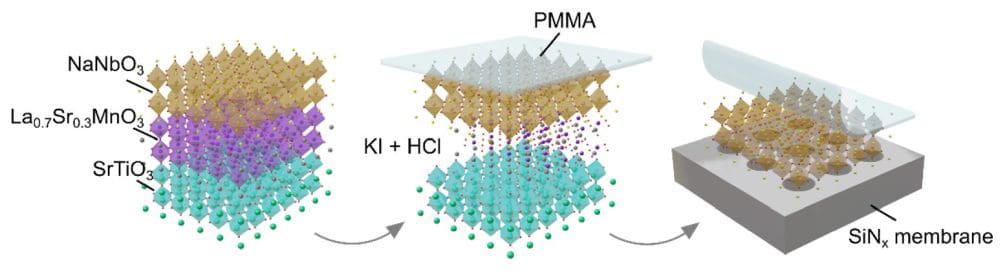
[Image above] Schematic illustrating the lift-off process for NaNbO3 thin films. By dissolving the La0.7Sr0.3MnO3 buffer layer in a mixed KI and HCl solution, the NaNbO3 thin film is released and transferred onto a 200-nm-thick SiNx membrane with arrays of holes in a diameter of 2–10 μm. Credit: Xu et al., Advanced Materials (CC BY 4.0)
Almost 70 years since Albert Einstein’s death, physicists are still chasing a “theory of everything,” i.e., an overarching hypothetical framework that would explain the physics of the entire universe in a single equation. The reason this search is so exasperating is because matter appears to behave very differently on the largest and smallest scales, and finding an equation that can explain both extremes has so far proven impossible.
Though exasperating for physicists, the material properties that emerge on very small scales are exciting for materials scientists. Industries from agriculture to computing are expected to benefit from the ongoing nanoscience and nanotechnology revolution.
Ferroelectric materials are one class of materials that have been extensively studied regarding size effects. Ferroelectricity is the property of certain materials to have spontaneous electric polarization that is reversible through application of external electric fields.
The spontaneous electric polarization in ferroelectrics allows these materials to exhibit something called negative capacitance behavior, which some researchers believe will revolutionize how electronics are miniaturized in the future.
On the other hand, there are far fewer studies on how structure and properties evolve in antiferroelectric materials with reduced dimensions.
Antiferroelectric materials are similar to ferroelectric materials in that both consist of an ordered (crystalline) array of electric dipoles. However, adjacent dipoles in antiferroelectrics are oriented in opposite directions, causing them to cancel each other out and resulting in no polarization on the macroscale. In contrast, ferroelectric dipoles all point in the same direction, resulting in macroscopic polarization.
An electric field of sufficient magnitude can induce antiferroelectrics to undergo a phase transition to a ferroelectric phase (i.e., parallel dipole ordering). This behavior makes antiferroelectrics of interest for use in high-energy density capacitors.
Understanding the size effects in antiferroelectrics would allow for their optimized use in miniaturized electronics. So, a group of researchers from several universities and national laboratories in the United States and France investigated these effects, and their open-access paper reports a surprising discovery.
Traditionally, gathering data on size effects in antiferroelectrics is complicated by how antiferroelectric thin films are made. The films are grown on commercially available substrates with different lattice structures. Lattice mismatch between the substrate and the thin film strains the antiferroelectric, so decoupling the strain effects from the size effects is challenging.
To overcome this challenge, the researchers introduced a sacrificial buffer layer between their lead-free sodium niobate (NaNbO3) thin film and substrate. This buffer layer allowed the film to be detached from the substrate after it was grown to the desired thickness.
Once detached, the researchers used a variety of experimental approaches to assess the strain-free films at thicknesses ranging from 9 nm to 164 nm.
Piezoresponse and optical measurements revealed that when the NaNbO3 films are thinner than 40 nm, they become completely ferroelectric. For thicknesses above 40 nm, the films contain a mixture of antiferroelectric and ferroelectric regions. But if a sufficient electric field is applied, the antiferroelectric regions undergo a nonreversible transition to ferroelectric, resulting in a completely ferroelectric thin film at thicknesses up to 164 nm.
These unexpected results prompted the researchers to use first-principles calculations to determine what drives the antiferroelectric-to-ferroelectric transition. They determined that surface effects—specifically, the c/a ratio—is the main cause.
The c/a ratio is a way to describe the shape of a lattice. The higher the ratio, the more distorted the lattice structure.
When film thickness decreases, there is a higher c/a ratio, and this structural distortion helps stabilize the ferroelectric phase. In contrast, a thicker film features a lower c/a ratio, which favors the antiferroelectric phase.
The researchers caution that many factors were not accounted for in the first-principles calculations, such as the presence of structural defects or inhomogeneities. As such, agreement between experiments and theory should be considered qualitative rather than quantitative.
They also mention the possibility that the ferroelectric phase is a result of the synthesis process.
“Note that the Pbcm antiferroelectric phase is more stable than the ferroelectric Pmc21 phase when NaNbO3 is unstrained. Therefore, the ferroelectric phase is favored in the as-grown NaNbO3 on SrTiO3 [the substrate],” they write.
“The relaxation from the strained ferroelectric phase to the unstrained antiferroelectric phase would require overcoming an energy barrier … If such an energy barrier increases in thin membranes due to dimensionality or surface effects, the thin membranes could remain frozen in their initial ferroelectric state during the lift-off process,” they add.
In an email, lead author Ruijuan Xu, assistant professor at North Carolina State University, says they are now working on fabricating NaNbO3-thin-film-based capacitors to probe electrical properties on the macroscale.
“We hope to achieve the ability to manipulate the phase stability and obtain enhanced electrical properties in NaNbO3 capacitors, which will be useful for potential applications,” she says.
The open-access paper, published in Advanced Materials, is “Size-induced ferroelectricity in antiferroelectric oxide membranes” (DOI: 10.1002/adma.202210562).