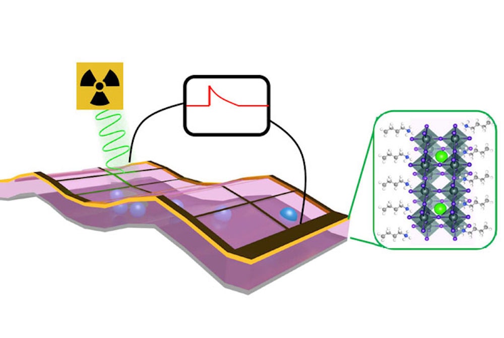
[Image above] Researchers from Los Alamos and Argonne National Laboratories developed X-ray detectors using 2D perovskite thin films that are a hundred times more sensitive than conventional silicon-based detectors. Credit: Los Alamos National Laboratory
When I hear the term “perovskite,” I immediately think of solar cells.
In the past decade, the efficiency of perovskite solar cells rose dramatically, from about 4% in 2009 to just over 25% in 2019. Research on these cells continues to expand rapidly, and we cover highlights from such research here on CTT (check out our most recent one from February).
Though solar cells are the most well-known application of perovskite materials, it is by no means the only application. To understand these materials’ potential, let’s take a quick look at their properties.
Organic-inorganic perovskites and 2D Ruddlesden− Popper
The term “perovskite” describes compounds with the same type of crystal structure as calcium titanium oxide, the mineral traditionally referred to as perovskite.
Most perovskite materials researched today are hybrid organic-inorganic lead or tin halide-based, which gives them unique properties.
“Perovskites offer a combination of the characteristics of inorganic and organic semiconductors: the chemical tunability of their optoelectronic properties and low-temperature and solution-based deposition recall organics; their relatively high carrier mobility, diffusion length, and radiative lifetime more resemble those of polycrystalline semiconductors,” researchers write in an MRS Communications article.
Organic-inorganic halide-based perovskites have a big downside, though—their 3D structure suffers from poor stability against humidity and photoirradiation. This downside has led to interest in 2D Ruddlesden−Popper perovskites.
2D Ruddlesden−Popper perovskites exhibit the majority of key photovoltaic properties of 3D perovskites while demonstrating higher stability. In particular, the composition (BA)2(MA)n−1PbnI3n+1 has received particular attention [BA = CH3(CH2)3NH3 and MA = CH3NH3].
Though initial research on perovskite materials focused on the energy field, rapid improvement of these materials in photovoltaic applications over the past decade has caught the attention of scientists in other fields, sparking research there as well.
Perovskites for medical imaging
In a recent study, researchers at Los Alamos National Laboratory and Argonne National Laboratory (ANL) used the 2D Ruddlesden-Popper perovskite (BA)2(MA)2Pb3I10 to create a new X-ray detector prototype that could lower the risk of radiation damage in medical imaging.
X-ray imaging is used for numerous routine exams, including dental exams and mammography. And as with other types of medical imaging, X-ray imaging presents a risk of cell damage from radiation exposure. Imaging with lower X-ray doses would lower the risk of damage, but that requires a detector that can detect a lower dosage.
The Los Alamos and ANL researchers used a synchrotron beamline at ANL’s Advanced Photon Source to investigate if their 2D perovskites could serve as the basis for sensitive radiation detectors. And based on the results, it appears they would serve this application well.
The 2D perovskite detector resulted “in a hundred times more sensitivity than conventional silicon-based detectors,” a Los Alamos press release explains. Specifically, the 2D perovskite detector sensitivity was up to 0.276 C Gyair−1 cm−3, compared to 0.000333 C Gyair−1 cm−3 for the silicon diode used in the study.
The researchers also found the perovskite detector does not require an outside power source to produce electrical signals in response to X-rays, which enables it to operate as a self-powered detector. However, with the addition of a small voltage source, they found thicker films work well too, which suggests the perovskite detector’s “useful energy range could be extended beyond X-rays to low-energy gamma-rays,” the press release adds.
The perovskite detectors offer one more advantage to silicon-based detectors—they can be produced with low-cost fabrication techniques.
“Potentially, we could use ink-jet types of systems to print large scale detectors,” Hsinhan Tsai, Oppenheimer Distinguished Postdoctoral Fellow at Los Alamos, says in the press release. “This would allow us to replace half-million-dollar silicon detector arrays with inexpensive, higher-resolution perovskite alternatives.”
The paper, published in Science Advances, is “A sensitive and robust thin-film X-ray detector using 2D layered perovskite diodes” (DOI: 10.1126/sciadv.aay0815).