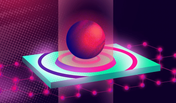
[Image above] Artistic rendering of the proposed quantum dot and graphene scheme developed by Russian researchers to improve conversion efficiency of light into surface plasmon polaritons. Credit: Daria Sokol, MIPT Press Office
When I discuss studies that involve nanoscale design, I often focus on studies that explore new fabrication processes or techniques that provide more control over the design of nanoscale structure.
But materials are not the only thing that scientists look to manipulate on the nanoscale. Light, or electromagnetic radiation, also is something scientists want to control because it opens up new and improved applications, such as biological analysis of molecules at the nanometer level.
Surface plasmon polaritons (SPPs) are one way that scientists harness light for use on the nanoscale. SPPs are a type of surface wave that exist at the interface between a conductive material, such as a metal, and a dielectric material, such as air. The waves consist of free electrons in the conductive material (surface plasmons) coupled with electromagnetic waves in the dielectric material, and they propagate together along the conductive–dielectric interface.
Compared to incident light, SPPs are shorter in wavelength. So harnessing SPPs to analyze a sample on the nanometer scale improves absorption and scattering signals on the sample’s small cross-section.
In a CTT post I wrote in July, I noted that scientists are interested in using 2D materials as the conductive material in an SPP system because 2D materials can support SPPs with shorter wavelengths, a phenomenon that allows analysis of smaller samples. However, what I did not discuss was the efficiency at which scientists can convert incident light on 2D surfaces into SPPs.
“The existing schemes for converting light to SPPs on 2D surfaces have an efficiency of no more than 10%,” a Moscow Institute of Physics and Technology press release explains.
It is possible that conversion efficiency can be improved by using intermediary signal converters, or nano-objects of various chemical compositions and geometries. So that is what researchers at MIPT and Vladimir State University in Russia looked to do in their recent simulation study.
The researchers explored using quantum dots as their intermediary signal converters. Quantum dots are semiconducting nanoscale particles that exhibit optical and electronic properties that differ from larger particles due to quantum mechanics.
Under certain conditions, a strong coupling emerges between quantum dots and a 2D surface, allowing nearly all of the energy of the quantum dots to convert into surface waves. In addition, the strong coupling opens up new possibilities for light manipulation on the nanoscale, such as nanolasing, photochemistry, and quantum entanglement. Thus, there are multiple reasons nanoscale researchers are interested in using quantum dots as intermediary signal converters.
The MIPT and Vladimir State researchers have conducted previous studies on the nonlinear interaction between SPP modes propagating along graphene waveguides integrated with quantum emitters, such as quantum dots and nanowires. However, in the recent study, “we dig the subject profoundly and in more detail with a strong focus on the light-QD [quantum dot]-SPP interaction,” Valentyn S. Volkov, director of the Center for Photonics and 2D Materials at MIPT and head of the Laboratory of Nanooptics and Plasmonics, says in an email.
The researchers used ellipsoid-shaped quantum dots made from indium antimonide (InSb) that were 40 nm in diameter. In their simulations, they arranged the quantum dots on top of a 2-nm silica buffer layer, which serves as a thin separator between the dots and the graphene surface.
In an email, Alexei Prokhorov, senior researcher at the MIPT Center for Photonics and 2D Materials and associate professor at Vladimir State University, explains why they included a buffer layer.
“Besides exciting surface waves, some of the QD energy is spent on trivial heat losses due to phonon mode excitation in the system. If the distance [between the quantum dots and surface] is too small—and certainly if the QD is in contact with the surface—the effect of dissipation becomes dominant,” Prokhorov says. Thus, to improve coupling between the quantum dots and the 2D surface, they must be separated by a small distance.
Using the simulations, the researchers determined an optimal arrangement for the quantum dots and graphene to achieve a strong coupling, which allowed a hybrid interaction to take place among the quantum dots, incident light, and SPPs.
“[The] quantum dot positioned above graphene interacts both with incident light and with the surface electromagnetic wave, but the frequencies of these two interactions are different. The dot interacts with light at a wavelength of 1.55 micrometers and with the surface plasmon-polariton at 3.5 micrometers,” Prokhorov says in the press release.
The researchers calculated the conversion efficiency of their setup to be as high as 90%–95%. When all potential negative factors that might affect this efficiency were accounted for, such as decreased chemical potential of graphene, the conversion efficiency remained above 50%—still several times higher than any other competing system.
Volkov says they are now working on the experimental realization of this system.
The paper, published in Laser & Photonics Reviews, is “Hybrid schemes for excitation of collective resonances with surface plasmon polaritons in arrays of quantum dots in the proximity of graphene” (DOI: 10.1002/lpor.202000237).