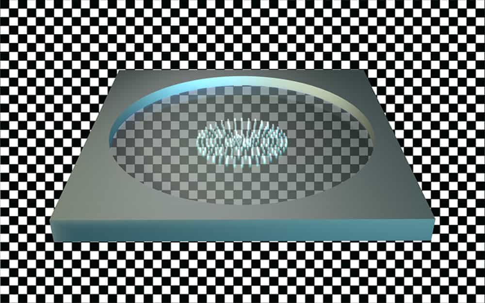
[Image above] Illustration of a metalens that uses holes rather than pillars to focus light. Credit: Lim et al., Nano Letters (CC BY-NC-ND 4.0)
Ever since the first official trailer for The Matrix Resurrections released on September 9, I’ve seen a lot of critics debating what appears to be a highly meta plot.
Meta is a prefix of Greek origin that can be used to mean a number of things, including “after,” “among,” “altered,” or “beyond.” In today’s society, “meta” is often used to signify self-reflection. For example, metadata is a set of data that describes and gives information about other data.
However, use of “meta” for only self-reflection or self-referential purposes is a limitation of the original Greek word. The current usage is due to a misinterpretation of Aristotle’s book Metaphysics by Latin writers, who took the title to mean “the science of that which transcends the physical” rather than the literal translation “the book that comes after the book entitled Physics.”
Fortunately, the relatively new word “metamaterial” offers an example of how “meta” can be used per its original definition. Metamaterials are materials engineered to have properties beyond those that naturally occur. The word first appeared in literature in a seminal 2000 paper, and the word is now enormously widespread due to increased research on these materials.
Metalenses are a type of metamaterial that we’ve covered quite a bit on CTT. Metalenses are flat, engineered lenses that focus light without causing chromatic aberrations (a type of image distortion that conventionally requires multiple lenses to correct).
Traditionally, metalenses use nanoscale arrays of columns or fin-like structures to focus light. However, in a new open-access paper published this month, researchers at the Harvard John A. Paulson School of Engineering and Applied Sciences (SEAS) developed a metalens that uses very deep, very narrow holes instead.
In the paper, they explain that using holes to focus electromagnetic waves is not a new idea—early plasmonic metasurfaces relied on nanoholes or slits in thin sheets of metal. However, “The application of these devices was limited by absorptive ohmic losses and the lack of control over the full 2π phase delay for light … [due to] the small height-to-width aspect ratio of the fabricated [nanostructures], which was limited to 5:1 for plasmonic lenses,” the authors write.
Some groups explored high-refractive index dielectric nanopillars as an alternative to holes, and the promising results led to an explosion in studies using the pillar-based platform. However, researchers are now running into limits with this approach.
Specifically, taller pillars are needed to expand the phase control of incident light. Yet increasing the pillar height also increases the chances of the pillar falling or breaking during processing. Thus, the maximum aspect ratio routinely used for metalenses is 15:1 for titanium dioxide and 20:1 for silicon.
In the new paper, the SEAS researchers returned to the idea of holes to achieve higher aspect ratios. This decision may be surprising considering that small aspect ratios were a reason to move away from holes initially. However, the small aspect ratio seen in the earlier studies had more to do with the materials and manufacturing processes used than the limits of holes themselves.

a) Comparison between a free-standing pillar metasurface and a holey metasurface. b) Artistic representation of a holey metalens. Monochromatic light with wavelength of 1.55 μm is incident on a thin crystalline silicon membrane, into which more than 12.5 million via-nanoholes were etched. Credit: Lim et al., Nano Letters (CC BY-NC-ND 4.0)
To achieve larger aspect ratios, the SEAS researchers used electron beam lithography and reactive-ion etching to pattern 5-μm silicon membranes. The resulting ultradeep holes in the membranes approached aspect ratios of 30:1, which expanded control over “the confinement and propagation of light over a wide parameter space,” Maryna Meretska, co-first author and SEAS postdoctoral fellow, says in a SEAS press release.
The researchers note that because the metalenses were fabricated using conventional semiconductor industry processes and standard materials, the lenses could be manufactured at scale in the future. In addition, future studies could explore filling the holes with liquid crystals or nonlinear materials to allow dynamic control of the properties of light.
The open-access paper, published in Nano Letters, is “A high aspect ratio inverse-designed holey metalens” (DOI: 10.1021/acs.nanolett.1c02612).