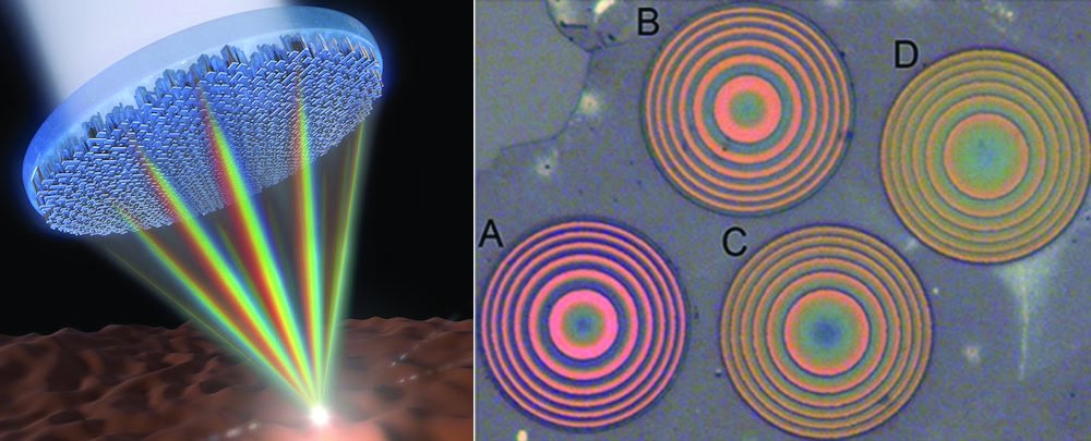
[Images above] Left, Harvard researchers focused the entire visible spectrum of light using a metalens; right, UW and National Tsing Hua University researchers developed metalenses thinner than the theoretical limit. Credit: Jared Sisler, Harvard SEAS; Liu et al., Nano Letters
It is a hard time for being a glass. First plastics took over as the preferred housing of carbonated beverages. Then polycarbonates decided to butt into the eyeglass and roofing markets. Yet glass still holds the lead among materials in cameras and imaging systems due to their high scratch resistance, optical clarity, and less image distortion.
But for how long?
Metasurface is a buzzword in optics research nowadays. A metasurface is a 2D sheet material made of an artificial nanostructured interface with subwavelength thickness, meaning the metasurface is thinner than the wavelength of the electromagnetic waves with which the surface interacts.
Researchers use metasurfaces to control microwaves and light waves, with the latter waves being of specific interest to optics researchers. Recently, optics researchers have been investigating a specific type of metasurface for light control: a metalens.
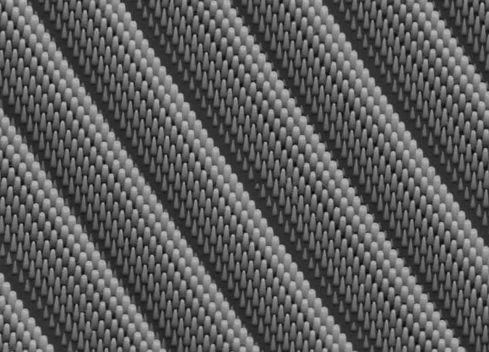
Metalenses are flat, engineered lenses constructed of nanoscale arrays of columns or fin-like structures. Because of their design, metalenses focus light without causing chromatic aberrations, a type of image distortion that conventionally requires multiple curved lenses of varying thickness to correct. If metalenses were used instead of glass lenses, there would be no need for multiple lens layers and the size of cameras and imaging devices could be greatly reduced.
Yet metalenses are not ready to hit the market just yet. Metalenses are limited in the spectrum of light they can focus well and are restricted in how small they can be created. For a metalens to achieve optimal imaging quality, the nanostructure arrays have to be roughly the same thickness as the wavelength of light they will focus.
Two studies this year made steps toward tackling these challenges. The first paper, published in January, was by researchers at the Harvard School of Engineering and Applied Sciences (SEAS). The second paper, published in October, came from a team of University of Washington and National Tsing Hua University researchers.
The Harvard SEAS researchers first demonstrated the efficiency of metalenses in 2016, but at that time could only focus one color at a time. In 2017 they succeeded in creating a metalens that could work within a continual bandwidth of colors—from blue to green—but the January study was the critical breakthrough. In this year’s paper, the Harvard SEAS researchers developed the first metalens that could focus the entire visible spectrum of light at one time. They achieved this feat by using paired nanofins to control the speed of different wavelengths of light simultaneously, resulting in all wavelengths reaching the focal spot at the same time.
Nine months after Harvard published their study, a team from the University of Washington and the National Tsing Hua University in Taiwan designed a solution to the nanostructure array thickness limitation.
Led by Chang-Hua Liu, a previous University of Washington postdoctoral researcher and now faculty member at the National Tsing Hua University, and senior author Arka Majumdar, a University of Washington assistant professor of physics and of electrical and computer engineering, the team published a paper describing how they constructed functional metalenses that are one-tenth to one-half the thickness of the wavelengths of light that they focus: about 190 nanometers thick. Their secret? Layered 2D materials.
“This is the first time that someone has shown that it is possible to create a metalens out of 2D materials,” says Majumdar in a press release (the Harvard SEAS researchers used titanium dioxide nanofins, not 2D materials, to create their metalens).
The UW and National Tsing Hua University team used widely studied van der Waals materials such as hexagonal boron nitride and molybdenum disulfide for the layers and then employed mathematical models originally formulated for liquid-crystal optics to achieve high efficiency despite the metalenses being thinner than the wavelengths they focused.
“These results open up an entirely new platform for studying the properties of 2D materials,” says Majumdar in the press release.
In addition to these studies furthering the possibility of using metalenses to replace traditional glass lenses, there is another reason to study metalenses. According to the University of Washington press release, metalenses can be easily transferred onto any substrate, including flexible materials, meaning research on metalenses paves the way toward flexible photonics.
The papers, published in Nature Nanotechnology and Nano Letters, are “A broadband achromatic metalens for focusing and imaging in the visible” (DOI: 10.1038/s41565-017-0034-6) and “Ultrathin van der Waals Metalenses” (DOI: 10.1021/acs.nanolett.8b02875).