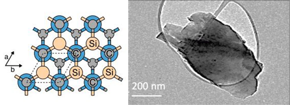
[Image above] (Left) Schematic depicting the honeycomb structure of monolayer silicon carbide. (Right) Transmission electron microscopy image of monolayer silicon carbide. Credit: (Left) Polley et al., Physical Review Letters (CC BY 4.0); (Right) Chabi et al., Nanomaterials (CC BY 4.0)
Silicon carbide is well-known in the ceramics world for its exceptional mechanical properties. Its combination of high hardness, high strength, and low density is almost second to none.
The possibility of replicating these properties in two dimensions is of great interest to researchers. But synthesizing 2D silicon carbide has proven to be a huge challenge, due in part to the different chemical bonding preferences between silicon and carbon.
As noted in a previous CTT on 2D materials, carbon naturally forms in flat, layered structures when bonding with itself (sp2 hybridization). In contrast, silicon prefers to bond in buckled or corrugated shapes (sp3 hybridization).
First-principles calculations predict that sp2 bonded (planar) silicon carbide is not only possible but should be the most energetically favorable configuration for this material in two dimensions. However, most experimental attempts to date on synthesizing 2D silicon carbide did not achieve the idealized honeycomb structure (see here, here, and here).
That is because multilayer nanosheets—even just a bilayer—resemble the bulk silicon carbide structure, which consists of sp3 bonding. Only a true monolayer of silicon carbide can form the stable planar structure.
Two recent papers successfully achieved monolayer silicon carbide. And they did so, as described below, through two completely different approaches.
Top-down synthesis of monolayer silicon carbide
In July 2021, researchers at the University of New Mexico published an open-access paper describing a top-down method for synthesizing monolayer silicon carbide.
The trick with using a top-down approach is that bulk silicon carbide features sp3 bonding. As such, there needs to be a phase transformation from sp3 to sp2 bonding to isolate a monolayer of silicon carbide.
To achieve this transformation, the researchers exfoliated hexagonal bulk silicon carbide in isopropyl alcohol or N-methyl-2- pyrrolidone using bath sonication for 24 hours. They then centrifuged the dispersion at an average rate of 1,000 rpm for about 5 minutes.
Drops of the silicon carbide dispersion were placed on different substrates, such as a holey carbon grid or silicon substrate, and dried at ambient conditions prior to characterization with electron microscopy and Raman spectroscopy, for example.

(a) Photographs of the exfoliation process and the dispersed silicon carbide. (b) Optical microscopy image of the monolayer silicon carbide nanosheets. Credit: Chabi et al., Nanomaterials (CC BY 4.0)
Characterization of the drops confirmed that the monolayer silicon carbide had a stable planar structure. Additional analysis of the material’s optical properties showed that the nanosheets had strong emission in the visible range.
“These results indicate that 2D SiC may be used for blue-green luminescent devices, e.g., light emitting diodes, as well as integrated micro/nano electronic circuits, such as LED integrated computer chips and biolabeling and biosensing,” the researchers conclude.
The open-access paper, published in Nanomaterials, is “The creation of true two-dimensional silicon carbide” (DOI: 10.3390/nano11071799).
Bottom-up synthesis of monolayer silicon carbide
In February 2023, researchers from Lund University, Chalmers University of Technology, and Linköping University in Sweden published an open-access paper describing a bottom-up method for synthesizing monolayer silicon carbide.
Their process began with a 360-µm-thick silicon carbide wafer, on which they sputtered a less-than-3-nm-thick film of either tantalum carbide or niobium carbide. The covered wafer was then annealed at 1,700ºC for 10 minutes.
During the annealing process, the silicon and carbon atoms from the wafer migrated to the surface of the carbide system and rearranged to form a stable, planar monolayer of silicon carbide. This structure, which was confirmed via spectral measurements, remained stable at temperatures up to 1,200ºC under vacuum conditions.

(a) Topographic scanning tunneling microscopy image of monolayer silicon carbide on a tantalum carbide surface. (b) Representative low-energy electron diffraction image; 2.32 Å−1 unit cell reciprocal vectors are indicated. (c) Schematic depiction of the sample structure. (d) Cross-sectional high-angle annular dark-field scanning transmission microscopy image of the tantalum carbide/silicon carbide interface. Credit: Polley et al., Physical Review Letters (CC BY 4.0)
Currently, the monolayer silicon carbide cannot be removed from the underlying bulk material because it interacts strongly with the metal carbide layer that it sits on. The researchers note that future experiments will likely investigate ways to decouple the monolayer silicon carbide from the substrate.
The open-access paper, published in Physical Review Letters, is “Bottom-up growth of monolayer honeycomb SiC” (DOI: 10.1103/PhysRevLett.130.076203).