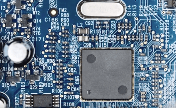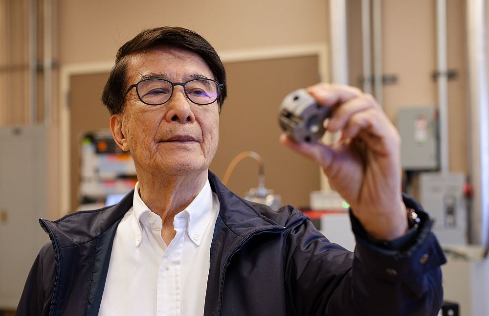
[Image above] Credit: University of Kentucky; YouTube
Graphene has a lot going for it.
The material’s single-layer thickness, toughness, and supreme mechanical and thermal properties make it an ideal choice for developing electronic, optoelectronic, and electromechanical devices and sensors.
Lately, graphene’s been making waves in the lab as researchers race to find the most applicable-yet-scalable way to use this wonder material.
- It effectively teams up with glass to boost electronic properties.
- It’s a metal that behaves like water.
- It interacts safely with brain neurons, which broadens its biomedical applications.
But now there’s a new one atom-thick material on the scene that could boot graphene from its seat as the wonder material to advance electronic tech as we know it.
A physicist at the University of Kentucky (Lexington, Ky.), working in collaboration with scientists from Daimler in Germany and the Institute for Electronic Structure and Laser (IESL) in Greece, has discovered a new material “made up of silicon, boron and nitrogen—all light, inexpensive, and earth abundant elements,” according to a university news release. To boot, this material is extremely stable—a property many other graphene alternatives lack.
Check out this video produced by the University of Kentucky that features senior author Madhu Menon’s explanation of the new material and how it could upstage graphene.

Credit: University of Kentucky; YouTube
“We used simulations to see if the bonds would break or disintegrate—it didn’t happen,” Menon, physicist in the University of Kentucky Center for Computational Sciences, says in the release. “We heated the material up to 1,000 degrees Celsius and it still didn’t break.”
Graphene’s strength and unique properties puts the material in a class of its own, but it has a downside: it isn’t a semiconductor and, because of that, it hasn’t been able to compete in the digital tech industry, the release explains.
Researchers on the quest to discover new 2-D semiconducting materials have relied on a class of three-layer materials called transition-metal dichalcogenides (TMDCs), which can be successfully made into digital processors. But TMDCs present significant bulk compared to wafer-thin graphene—and they’re made of materials that aren’t readily available or necessarily cheap.
Menon and his colleagues set their sights on finding an alternative that is light, earth-abundant, inexpensive, and can act as a semiconductor. After many tests and experiments, they uncovered the right combination of silicon, boron, and nitrogen to create a stable structure that was arranged in the same hexagonal molecular pattern as graphene.
While the new material is metallic like graphene, it can be transformed into a semiconductor easily by attaching other elements on top of the silicon atoms—a property that offers the “exciting possibility of seamless integration with the current silicon-based technology,” the release explains.
And the attachment of other elements can also be used to selectively change band gap values—a major advantage over graphene when it comes to solar energy conversion and electronics applications, according to the research.
“We are very anxious for this to be made in the lab,” Menon says. “The ultimate test of any theory is experimental verification, so the sooner the better!”
The paper, published in Physical Review B, Rapid Communications, is “Prediction of a new graphene-like Si2BN solid” (DOI: 10.1103/PhysRevB.93.081413).
Author
Stephanie Liverani
CTT Categories
- Electronics
- Material Innovations


