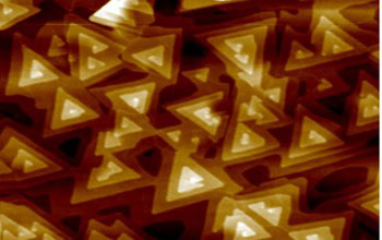
[Image above] The surface of a bismuth selenide film shows the triangular layer structure that is characteristic of 2-D chalcogenide materials. Credit: Joan Redwing, Department of Materials Science and Engineering, Penn State University
It looks like 2016 could be the year of new materials.
The January/February issue of the ACerS Bulletin’s cover article features DARPA’s Materials Development for Platforms—a new program that aims to speed up new materials development with a fresh, application-driven approach to innovation.
At the end of February, the U.S. Department of Energy launched a $40 million effort to improve materials for clean energy solutions.
And many science agencies can expect to see their federal budgets return to levels not seen since the fiscal year 2013 sequestration in FY 2016, even adjusting for inflation, according to the American Association for the Advancement of Science.
It’s safe to say the money is flowing for new-and-improved materials R&D this year.
Last week, a new Materials Innovation Platforms (MIP) program funded by the National Science Foundation made its first awards to Penn State University and Cornell University, with the aim to “significantly accelerate materials research and development,” according to a recent NSF news release.
The institutions will serve as “platforms” to develop new bulk and thin-film crystalline hard materials through state-of-the-art instrumentation in an environment that “combines multidisciplinary expertise with the best tools available, providing access to the instrumentation, data, and new materials created,” the release explains.
- Penn State University will focus on developing new materials for next-generation electronics that are faster, use less energy, and can be built on flexible substrates, as well as other applications at its new facility, the 2-D Crystal Consortium (2DCC).
- Cornell University will focus on the interfaces between oxide-based and 2-D materials with its Platform for the Accelerated Realization, Analysis, and Discovery of Interface Materials (PARADIM).
“We see the platforms as pushing the frontiers in materials research,” Fleming Crim, NSF assistant director for mathematical and physical sciences, says in the release. “In its first call for proposals, NSF is focusing on crystal growth because the U.S. has fallen behind in this area of science after having been a global leader in material synthesis, which is essential for advancing basic materials research and will add to the important investment the foundation is making in mid-scale instrumentation.”

Cylindrical single crystals of strontium holmium oxide and titanium oxides, examples of new interface materials that can be created by users of PARADIM. Credit: PARADIM; Cornell University
The MIP program was inspired by the Materials Genome Initiative, which was launched in 2011 to “discover, manufacture, and deploy advanced materials in half the time and at a fraction of the cost,” the release explains.
MIP program awardees will each act as a “nexus of activity” for a focused research theme, where platforms are equipped with user facilities, according to the release. Researchers throughout the U.S. who also engage in these area of research will have access to the resources, too, to help get their own work on the fast track to development.
“Without question, one of the most exciting aspects to these awards will be to see just how quickly these platforms can accelerate the pace of materials development,” Sean L. Jones, NSF materials research program director, says in the release. “The awards are fairly complementary to one another and accelerate research in two distinct material systems likely to have a significant impact on technology as they transform the field at the most fundamental level.”
For more information, visit NSF’s MIP website.