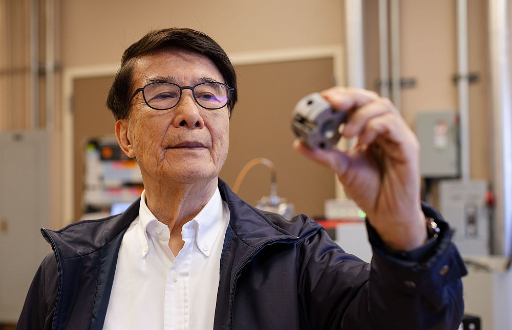
[Image above] Polycrystalline film growth during coevaporation in real time using in situ X-ray diffraction and fluorescence analysis. Credit: R. Mainz, C.Kaufmann/HZB.
Photovoltaic cells based on thin films of copper indium gallium selenide are among the most promising and efficient PV technologies, and coevaporation is a common technique used for CIGS cell fabrication. The process involves simultaneous evaporation of indium or gallium, copper, and selenium to produce a thin crystalline film with minimal defects.
“Until recently, we did not fully understand what exactly happens during this coevaporation process,” said Roland Mainz of Helmholtz Zentrum Berlin Institute of Technology (Germany) in a news release. Mainz and his research team worked for three years to solve this riddle before hitting on a technique that allows real-time observation of chalcopyrite formation in CIGS thin films.
Scientists knew that the thin films at the heart of CIGS PV cells have the chalcopyrite crystal structure. Copper deficiency in the material allows electrons to flow to the copper vacancies, resulting in conversion efficiencies that may exceed 20 percent. But it took a novel experimental chamber and exposure to synchrotron light at HZB’s BESSY II electron storage ring to give researchers a roadmap to coevaporation process optimization.
HZB’s chamber contained evaporation sources for the CIGS elements, plus heating and cooling elements that allowed the researchers to control coevaporation. “One of the main challenges was adjusting the chamber, which weighs around 250 kg, with an accuracy of 10 μm,” Mainz said in the release, explaining that thermal expansion of the film during evaporation requires automatic height adjustment every few seconds.
According to the release, the setup allowed Mainz and his team to observe real-time polycrystalline film growth during coevaporation using in situ X-ray diffraction and fluorescence analysis. “We are now able to see how crystalline phases form and transform, and when defects form during the different stages of evaporation,” Mainz explained. “But we’re also able to tell when these defects disappear again.”
According to the release, defects start to diminish in the second stage of coevaporation, during deposition of copper and selenium. Mainz said excess copper deposits at the film surface in the form of copper selenide to help reduce defects. “This was already known before from previous experiments. But now, using fluorescence signals and numeric model calculations, we are able to show how copper selenide penetrates the copper indium selenide layer,” he explained.
“We now know that for further optimization of the process it is important to concentrate on the transition point into the copper-rich phase. Up to now the process was performed very slowly throughout all stages to give defects enough time to disappear. Our findings suggest that the process can be accelerated at some stages and that it is sufficient to slow it down only at points where defects are efficiently eliminated,” he concluded.
Results of the work were recently reported in a paper in Advanced Energy Materials (DOI: 10.1002/aenm.201300339).
Author
Jim Destfani
CTT Categories
- Basic Science
- Energy


