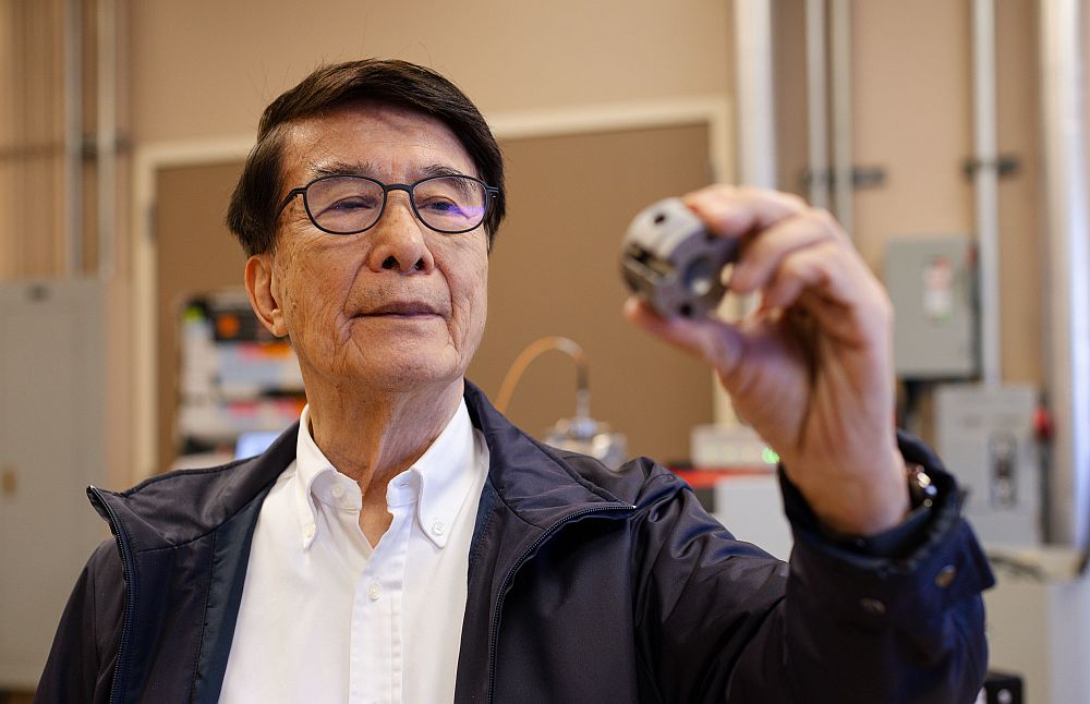
[Image above] Credit: NIST
The University at Buffalo has launched the Department of Materials Design and Innovation, a forward-leaning, interdisciplinary initiative that will address demand for new materials. The department is possible thanks to Buffalo alumnus and ACerS honorary member Erich Bloch’s generous donation of $1.5 million for an endowed chair to lead the new department.
‘Forests’ of carbon nanotubes grown on 3D substrates
A team of University of Maryland researchers is growing vertically aligned “forests” of carbon nanotubes on 3D conductive substrates to explore their potential use as a cathode in next-gen lithium batteries. The nanotubes are grown on a porous, “sponge-like” foam structure made of nickel coated with aluminum oxide ceramic.
ORNL materials researchers get first look at atom-thin boundaries
Scientists at the DOE’s Oak Ridge National Lab have made the first direct observations of a 1D boundary separating two different, atom-thin materials. Theorists have predicted the existence of intriguing properties between two crystalline components, but experimental verification had previously eluded researchers.
Study at SLAC explains atomic action in high-temperature superconductors
A study at the DOE’s SLAC National Accelerator Laboratory explains why a thin layer of iron selenide superconducts at much higher temperatures when placed atop a material composed of strontium, titanium, and oxygen. The study suggests how to engineer superconductors that work at higher temperatures.
New process isolates thin sheets of molybdenum disulfide
Researchers at Northwestern University are studying how to isolate atomically thin sheets of molybdenum disulfide at a larger scale. To do so, researchers have developed methods for exfoliating thin layers of graphene from graphite using solution-based methods.
New form of crystalline order holds promise for thermoelectric applications
A team of researchers from Vanderbilt University and Oak Ridge National Laboratory has discovered an entirely new form of crystalline order, which simultaneously exhibits both crystal and polycrystalline properties, or “interlaced crystals,” in nanoparticles of copper-indium sulfide.
Lawrence Livermore develops method to measure residual stress in 3-D printed metal parts
Lawrence Livermore National Lab researchers have developed an efficient method to measure residual stress in metal parts produced by powder-bed fusion additive manufacturing. The residual stress measurement method combines traditional stress-relieving methods (destructive analysis) with modern technology: digital image correlation.
Revolutionary solar-friendly form of silicon shines
A team of Carnegie scientists has synthesized an entirely new form of silicon that has a quasi-direct band gap that falls within the desired range for solar absorption. The silicon is a so-called allotrope that consists of an interesting zeolite-type open framework.