[Image above] Credit: NIST
NANOMATERIALS
How to tell when a nanoparticle is out of shape: Method ensures well-rounded measurements
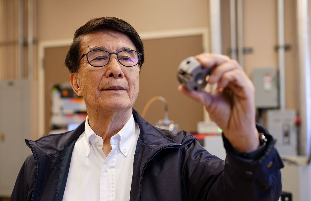
NIST scientists show that when the same set of nanoparticles is measured with the two most widely used reference methods, calculated volume estimates can differ by as much as 160%. The researchers have proposed and tested a novel combined measurement scheme that can minimize errors while still maintaining high measurement throughput.
Advance in intense pulsed light sintering opens door to improved electronics manufacturing
Taking a deeper look at photonic sintering of silver nanoparticle films, scientists at Oregon State University have uncovered a relationship between film temperature and densification. The engineers found a temperature turning point in intense pulsed light despite no change in pulsing energy, and discovered that this turning point appears because densification reduces the nanoparticles’ ability to absorb further energy from the light.
Going green with nanotechnology
Nanotechnology can be applied to save raw materials and energy, develop enhanced solar cells and more efficient rechargeable batteries, and replace harmful substances with eco-compatible solutions. For three years, the Bavarian State Ministry for the Environment and Consumer Protection had financed the association consisting of ten individual nanotechnology projects.
ENERGY
Experiments allow in situ analysis of water management to improve fuel cells
Scientists are exploring water management in an alternative proton exchange membrane type, called PFIA. Experiments have been conducted using the infrared facilities of a synchrotron to explain why PFIA membranes are superior to the widely used NAFION membranes at higher temperatures and low humidity.
New approach captures the energy of slow motion
A new concept in energy harvesting could capture energy currently wasted and use it to power next-generation electronic devices, according to a team of Penn State scientists. The project, funded by Samsung, designed a mechanical energy transducer based on flexible, organic, ionic diodes that points to scalable energy harvesting of unused mechanical energy.
Researchers model the way into a nuclear future
Physicists from Moscow Institute of Physics and Technology and the Russian Academy of Sciences described the mobility of line defects, or dislocations, in uranium dioxide. This will enable future predictions of nuclear fuel behavior under operating conditions.
Researchers fabricate high performance Cu(OH)2 supercapacitor electrodes
A team of scientists at the University of Tehran have used an ultra-fast and simple method for fabrication of different types of copper-based nanostructures. By applying electric field in the ammonium hydroxide based solutions dense arrays of copper based nanostructures in short duration of time in the order of below 1 min have been achieved.
BIOMEDICINE
Better material for bone tissue regeneration
A new study from Tomsk Polytechnic University has revealed a technology how to cover biodegradable implants with a human skeleton similar mineral. The scientists have developed a new vaterite-based coating for nanofiber material used as scaffold to grow bone tissue cells in a shorter time. The process of porous calcium carbonate covering on electrospun PCL fibers was described in this study.
OTHER RESEARCH
Self-healing, transparent, highly stretchable material can improve batteries, electronics, more
Scientists, including several from the University of California, Riverside, have developed a transparent, self-healing, highly stretchable conductive material that can be electrically activated to power artificial muscles and could be used to improve batteries, electronic devices, and robots.
Miniscule amounts of impurities in vacuum greatly affecting OLED lifetime
Reproducibility is a necessity for science but has often eluded researchers studying the lifetime of organic light-emitting diodes. Recent research from Japan sheds new light on why: impurities present in the vacuum chamber during fabrication but in amounts so small that they are easily overlooked.
World’s first vertically stacked gate-all-around Si nanowire CMOS transistors
imec reported for the first time the CMOS integration of vertically stacked gate-all-around silicon nanowire MOSFETs. Key in the integration scheme is a dual-work-function metal gate enabling matched threshold voltages for the n- and p-type devices.
Energy cascades in quasicrystals trigger an avalanche of discovery
Quasicrystals have atomic structures that are geometrically organized but, unlike those of crystalline materials, never repeat themselves. In a new study from Argonne National Lab, scientists looked at networks of magnetic material patterned into these unique and quite beautiful geometries to see how nonrepeating patterns lead to the emergence of unusual energetic effects.
Author
April Gocha
CTT Categories
- Material Innovations
- Weekly Column: “Other materials”

