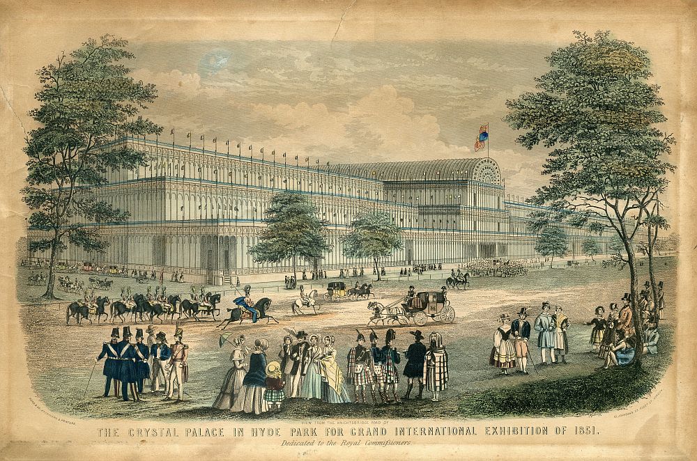
Ohio State officially opens new microscopy center
Ohio State University’s new Center for Electron Microscopy and Analysis, a $15 million facility featuring 10 FEI electron microscopes, has officially opened for business. Equipment at the center includes two aberration-corrected scanning transmission electron microscopes optimized to perform analysis on the atomic scale, three additional TEMs, two dual-beam focused ion beam instruments, and three scanning electron microscopes. There are also two X-ray diffractometer (XRD) systems, facilities for nanoindentation, and an extensive array of sample preparation facilities.
Schott offers high-homogeneity optical glasses from stock
Schott announced it will offer high-quality optical glasses up to H4 quality level from stock. The company says high-homogeneity glasses with a variety of compositions and shapes will be available with an extremely narrow variation in refractive index within individual pieces. Glass pieces in H4 quality have a maximum peak to valley refractive index variation of 2 × 10⁻⁶, while H5 quality glass has variation of 1 × 10⁻⁶ when tested in accordance with ISO 12123. According to Schott, glasses of this quality enable extremely high-resolution imaging and are suited for use in laser, measurement, semiconductor, and satellite applications. All products will be shipped with an individual test report produced using a special interferometer, the company says.
Room-temperature nanoparticle ceramics for electronics applications
(Materials views.com) Multifunctional electronics modules integrating passive components including electricity generation and storage are needed in next-generation smartphones smartphones and other electronics. Such components may consist of various ceramics and metal for wiring, and typical ceramic firing temperatures make it difficult to incorporate low-resistivity, low-melting-point metals such as copper in the devices. Researchers at Fujitsu Laboratories Ltd. developed a dense, thick, and organic-binder-free ceramic film consisting of stress-free nanoparticles that can be sintered at temperatures 500°C lower than those needed for bulk ceramics. According to Fujitsu, photolithography and wet etching for patterning and processing can be adapted to the thick ceramic green-state films, which have electrical properties identical to those of bulk ceramics.
New magnetic semiconductor material holds promise for spintronics
Researchers at North Carolina State University have created a new compound that can be integrated into silicon chips and is a dilute magnetic semiconductor—meaning it could be used to make spintronic devices, which rely on magnetic force to operate rather than electrical currents. The researchers synthesized the new compound, strontium tin oxide (Sr3SnO), as an epitaxial thin film on a silicon chip after setting out to create a topological insulator material—a material that is an insulator in bulk but has a highly conductive surface. Two materials—bismuth telluride and bismuth selenide—are known topological insulators, but scientists had predicted others, including Sr3SnO.
New technique for studying boundary regions in oxide superconductors
Researchers at the US Department of Energy’s Argonne National Laboratory studying the relationship between superconductivity and magnetism in superconducting materials have developed a new technique to study the boundary regions in oxide superconductors. Properties in regions near boundaries in these structures are not well understood, the scientists say, so they developed an approach that samples the behavior of electrons in boundary regions using especially sensitive scanning tunneling microscopy. The technique couples X-rays with scanning probes, reducing the time and cost required to analyze the behavior of these materials.