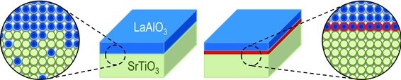
[Image above] Schematic of the structure of a typical lanthanum aluminate-strontium titanate interface, left, and the abrupt, sharp interface obtained through an atomic layer engineering method developed at ORNL. Credit: Choi et al.; Advanced Materials.
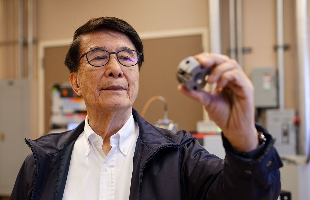
Oak Ridge National Lab researcher Ho Nyung Lee has studied complex-oxide thin films for over a decade, and during this time he particularly has been interested in exploiting the potential properties of functional complex-oxide perovskites thin films. Even more particularly, Lee leads a research team that has been striving to develop techniques to create perfect or nearly perfect thin films and superlattices by precisely controlling surfaces and interfaces. Now, in a newly published paper, Lee and his fellow researchers report they have been able to engineer a chemically stable and atomically sharp lanthanum aluminate monolayer (i.e., a perfect or nearly perfect interface) between LaAlO3 and strontium titanate heterostructures.
The core of the group’s findings is that a single unit cell layer of LaAlO3 grown on SrTiO3 substrate could serve as a buffer and is sufficient to dramatically improve the interface quality. In an ORNL press release, Lee says, “This means that we can now create new properties by precisely conditioning the boundary in the process of stacking different oxides on top of each other.”
The group’s general approach is to use pulsed laser deposition to grow the LaAlO3 on the SrTiO3 substrates at relatively low oxygen pressures. The breakthrough came when Lee and the others began to systematically examine how varying the oxygen pressure would affect the thin film structure. After looking at a wide range of pressures, their results showed an unexpected phenomenon: Relatively high oxygen pressure could initially produce a “shielding layer” of LaAlO3, and if this was followed by PLD growth at a lower pressure, the end result is a highly ordered, essentially defect-free interface.
One thing that appears to be very nice about this development is that the group reports this is not an isolated effect, and its atomic layering technique appears to be applicable to perovskite oxides in general.
This work also touches on a number of topics that have been organized under the umbrella of “The Grand Challenges of Ceramic Materials,” including the development of oxide electronics and gaining the ability to predict heterogeneous microstructures with unprecedented functionalities. Indeed, ceramists and other materials scientists are excited about the prospects of work, such as Lee’s. That is because designing and synthesizing oxide surfaces, interfaces and nanoscale structures could deliver a wide spectrum of electronic properties, including high mobility, superconductivity and magnetism, which could be tuned by external electrical, optical, magnetic, mechanical and chemical stimuli. Thus, its not surprising that Lee’s group expects its work to lead to the creation of novel materials with applications in energy and information technologies; more efficient solar cells, batteries and solid oxide fuel cells; faster transistors; and more powerful capacitors.
The group’s work is published in Advanced Materials, in a paper titled “Atomic Layer Engineering of Perovskite Oxides for Chemically Sharp Heterointerfaces” (doi:10.1002/adma.201202691).