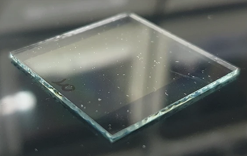
[Image above] Illustration of a graphene-based memristor, which was fabricated using a proprietary chemical vapor deposition method developed by Paragraf Limited. Credit: Weng et al., ACS Applied Electronic Materials (CC BY 4.0)
The electrification of industrial processes and the transportation sector both contribute to the growing global demand for electricity. But another key player in this growth is the expansion of data centers.
Data centers are physical facilities used to house computer systems and associated components, such as telecommunications and storage systems. With the adoption of artificial intelligence and machine learning computing processes, data center capacity must increase tremendously to handle the workloads of these advanced computing systems.
However, as the volume of data to be processed continues to expand, relying on traditional computing systems to process this data would result in exorbitant costs and substantial physical areas. So, new computing devices and architectures must be developed to process this data more efficiently.
Memristors are an emerging resistive switching memory device recognized as potential game-changers in computing. These passive, two-terminal devices are characterized by their ability to change resistance based on the history of the current or voltage previously applied. This behavior allows memristors to mimic biological synaptic functions in artificial neural networks, resulting in higher scalability and integration density, lower power consumption, and faster processing speeds than current field-effect-transistor technology.
The theory of memristive behavior was established around five decades ago, but it wasn’t until 2008 that they were first made in the laboratory. Modern memristors are typically sandwich structures consisting of an insulating active layer between two metal electrodes. There is a lot of research on different types of materials for the active layer, including metal oxides, organic materials, and low-dimensional nanomaterials. But there is also research on alternative materials for the electrodes, namely graphene.
Graphene electrodes for memristors have the benefits of flexibility, high transparency, high conductivity, high uniformity, and single-atom thickness. Because graphene is chemically and structurally stable, it prevents device degradation caused by oxygen vacancy and metal-ion diffusion. Graphene electrodes also show promise for photonic memristors because of their high transparency and supply chain sustainability compared to indium tin oxide, the material commonly used in this application.
Transitioning graphene electrodes into commercial memristor production, however, is hindered by challenges with producing large-area monolayer graphene on technologically relevant substrates. In a recent open-access paper, researchers from Queen Mary University of London and Paragraf Limited described a proprietary fabrication method based on chemical vapor deposition that could overcome this challenge.
The procedure, which was developed by Paragraf, allows for high-quality, monolayer graphene electrodes to be directly grown on sapphire substrates without any metal catalyst in batches of up to 37 wafers. It is already being used in commercial devices such as graphene-based Hall effect sensors and field-effect transistors. In the recent paper, the researchers extend the use of this procedure to memristor fabrication as well.
This development “paves the way for the realization of more powerful and compact integrated graphene electronics in the future,” the researchers write in the paper.
The open-access paper, published in ACS Applied Electronic Materials, is “Memristors with monolayer graphene electrodes grown directly on sapphire wafers” (DOI: 10.1021/acsaelm.4c01208).
Author
Laurel Sheppard
CTT Categories
- Electronics
- Manufacturing


